Unit 1 · 26 min read
Microprocessors and the Intel 8085
What the syllabus asks for 9
- What a microprocessor is
- A microprocessor system and its buses
- The 8085 at a glance
- The flag register
- Pins and signal groups
- Instruction cycle, machine cycle, T-state
- Interrupts (introduction)
- A first look at the 8086
- Seeing the ideas: real chips, buses, multiplexing, timing and flags
A microprocessor is a whole CPU on one chip. This unit builds the vocabulary — bus, register, ALU, flag, machine cycle — on the classic Intel 8085, a processor small enough to understand completely.
Everything later in the book (control units, pipelines, caches) is this same machine made faster.
- What a microprocessor is and how a microprocessor system is wired: CPU, memory, I/O and the three buses.
- The architecture of the 8085: registers, ALU, flags, timing and control, interrupts, pins.
- Instruction cycle, machine cycle and T-state, with the timing of the common cycles.
- A first look at the 8086 and why it was a step forward.
1.1 What a microprocessor is
A microprocessor is a programmable integrated circuit that fetches instructions from memory, decodes them and executes them.
Its three jobs: arithmetic and logic (the ALU), temporary storage (registers) and control (sequencing every step with timing signals).
A microcomputer adds memory and I/O around it; a microcontroller puts CPU, memory and I/O on one chip (a washing-machine controller, an Arduino's ATmega).
| Word size | Meaning | Examples |
|---|---|---|
| 4-bit | 4 data lines | Intel 4004 (1971) |
| 8-bit | 8 data lines, 16 address lines (64 KB) | 8080, 8085, Z80, 6502 |
| 16-bit | 16 data lines, 20 address lines (1 MB) | 8086, 8088 |
| 32/64-bit | modern PCs and phones | Pentium, Core, ARM |
The word length is the number of bits the ALU handles at once; it is also normally the width of the data bus.
1.2 A microprocessor system and its buses
A microprocessor system has four blocks joined by three buses:
- CPU — the 8085 itself.
- Memory — ROM (program that must survive power-off) and RAM (data and programs being run).
- Input/output devices — keyboard, display, sensors, via interface chips.
- Buses — groups of wires shared by all blocks.
| Bus | Direction | Carries | 8085 width |
|---|---|---|---|
| Address bus | one-way, CPU → others | the location (memory cell or I/O port) being accessed | 16 lines → 2¹⁶ = 65,536 locations (64 KB) |
| Data bus | two-way | the data or instruction being transferred | 8 lines → one byte at a time |
| Control bus | mixed | timing and command signals: RD', WR', IO/M', ALE, READY… | several lines |
To read a byte: the CPU puts the address on the address bus, activates the memory-read control signal, the addressed device places its byte on the data bus, and the CPU latches it. A write is the same with the CPU supplying the data.
The CPU is the bus master; memory and I/O are slaves.
1.3 The 8085 at a glance
The 8085 (Intel, 1976) is an 8-bit processor in a 40-pin package, needing a single +5 V supply. Features:
- 8-bit data bus; 16-bit address bus → 64 KB of memory; separate 256 I/O ports.
- On-chip clock generator: a 6 MHz crystal gives an internal 3 MHz clock (the 8085A-2 runs at 5 MHz).
- Five hardware interrupts plus eight software interrupts (RST n).
- Serial input and output lines (SID, SOD).
- 74 instructions, 246 opcodes; multiplexed address/data lines to save pins.
Functional blocks
| Block | Role |
|---|---|
| ALU | add, subtract, AND, OR, XOR, compare, rotate, increment, decrement; its inputs are the accumulator and a temporary register |
| Accumulator (A) | 8-bit register holding one operand and receiving the result |
| Temporary register | holds the second operand during an ALU operation; not programmer-visible |
| Flag register | five condition flags set by ALU results |
| General registers B, C, D, E, H, L | 8-bit, usable singly or as pairs BC, DE, HL |
| W, Z | internal temporary registers used by CALL, XCHG and similar; not programmer-visible |
| Program counter PC | 16-bit; address of the next instruction; incremented after each fetch |
| Stack pointer SP | 16-bit; address of the top of the stack in memory |
| Instruction register and decoder | holds the opcode just fetched and decodes it |
| Timing and control unit | generates all control signals in step with the clock |
| Interrupt control, serial I/O control | handle INTR/TRAP/RST lines and SID/SOD |
| Address buffer, data/address buffer | drive A8–A15 and the multiplexed AD0–AD7 |
The programmer's model
 A  (accumulator, 8)        Flags: S Z - AC - P - CY
 B   C    ← pair BC          PC  (16)   next instruction
 D   E    ← pair DE          SP  (16)   top of stack
 H   L    ← pair HL (also acts as the memory pointer "M")
M is not a physical register: it means "the memory byte addressed by HL". MOV A,M copies that byte into A. Many instructions can use M in place of a register, which is how the 8085 walks through arrays.
1.4 The flag register
An 8-bit register of which five bits are used. After most arithmetic and logic instructions the flags describe the result.
| Flag | Bit | Set (1) when |
|---|---|---|
| S Sign | D7 | bit 7 of the result is 1 (negative in two's complement) |
| Z Zero | D6 | the result is 0 |
| AC Auxiliary carry | D4 | carry from bit 3 to bit 4 (used by DAA for BCD) |
| P Parity | D2 | the result has an even number of 1 bits |
| CY Carry | D0 | carry out of bit 7 on addition, or borrow on subtraction; also set/cleared by rotate and compare |
Bits D5, D3 and D1 are unused. Flags let programs make decisions: JZ, JNC, JM and the other conditional jumps test them. Note that INR and DCR change S, Z, AC, P but not CY, and that data-transfer instructions (MOV, MVI, LDA…) change no flags.
9BH + 75H. 1001 1011 + 0111 0101 = 1 0001 0000. Result = 10H, so: CY = 1 (carry out of bit 7), Z = 0, S = 0 (bit 7 of 10H is 0), P = 0 (one 1-bit → odd), AC = 1 (low nibbles B + 5 = 10H carries).
3EH + 42H = 80H: S = 1, CY = 0, Z = 0, P = 0 (one 1 bit); the signed overflow (positive + positive = negative) is not flagged separately on the 8085 — you must notice S changing sign yourself.
05H − 05H = 00H: Z = 1, CY = 0 (no borrow), P = 1 (zero 1-bits is even). CPI 09H with A = 05H: A − 09H would borrow, so CY = 1, Z = 0, and A stays 05H (compare does not store the result).
1.5 Pins and signal groups
You are expected to know the groups, not memorise all 40 pin numbers.
| Group | Pins | Meaning |
|---|---|---|
| Address bus | A8–A15 | the high-order byte of the address, output only |
| Multiplexed bus | AD0–AD7 | low-order address byte and the data byte, at different times |
| ALE | 1 | Address Latch Enable: pulses high at the start of each machine cycle so an external latch (74LS373) can capture AD0–AD7 as A0–A7 |
| Status/control | IO/M', S0, S1, RD', WR' | tell whether the cycle is memory or I/O, and read or write; RD' and WR' are active low |
| Interrupts | TRAP, RST 7.5, 6.5, 5.5, INTR, INTA' | request lines and the acknowledge output |
| DMA | HOLD, HLDA | a DMA controller asks the CPU to release the buses; the CPU acknowledges |
| Wait | READY | a slow device pulls it low to make the CPU insert wait states |
| Reset | RESET IN', RESET OUT | RESET IN' low sets PC = 0000H |
| Serial | SID, SOD | serial input and output data |
| Clock | X1, X2, CLK OUT | crystal in; system clock out for peripherals |
| Power | Vcc (+5 V), Vss (ground) |
A 40-pin package cannot hold 16 address pins, 8 data pins and all the control pins. The 8085 therefore sends A0–A7 on AD0–AD7 first (with ALE high), then the same pins carry data.
A latch holds the low address byte so that the address stays valid while the pins turn into data lines. Demultiplexing = one 74LS373 latch enabled by ALE.
1.6 Instruction cycle, machine cycle, T-state
- T-state: one period of the processor clock — the smallest unit of timing. At 3 MHz, T = 1/3 µs = 0.333 µs.
- Machine cycle (M-cycle): one complete bus operation — opcode fetch, memory read, memory write, I/O read, I/O write, interrupt acknowledge — made of 3 to 6 T-states.
- Instruction cycle: everything needed to fetch and execute one instruction — one to five machine cycles.
Instruction cycle  = M1 (opcode fetch) + M2 + M3 …
Machine cycle      = T1 + T2 + T3 (+ T4 + T5 + T6)
The machine cycles and their status lines
| Machine cycle | IO/M' | S1 | S0 | T-states |
|---|---|---|---|---|
| Opcode fetch | 0 | 1 | 1 | 4 (6 for a few, e.g. PUSH, CALL, RST) |
| Memory read | 0 | 1 | 0 | 3 |
| Memory write | 0 | 0 | 1 | 3 |
| I/O read (IN) | 1 | 1 | 0 | 3 |
| I/O write (OUT) | 1 | 0 | 1 | 3 |
| Interrupt acknowledge | 1 | 1 | 1 | 3 |
Inside the opcode fetch cycle (4 T-states)
- T1: the CPU puts the PC on the address bus (high byte on A8–A15, low byte on AD0–AD7); ALE = 1 so the latch captures the low byte. PC is incremented.
- T2: RD' goes low; the memory begins to respond.
- T3: the opcode appears on AD0–AD7 and is loaded into the instruction register; RD' goes high.
- T4: the opcode is decoded; the ALU works if the instruction needs no further memory access.
For a memory read or write cycle, T1 outputs the address (ALE high), T2 asserts RD' or WR', T3 completes the transfer.
Counting machine cycles and T-states
| Instruction | Bytes | Machine cycles | T-states | Why |
|---|---|---|---|---|
MOV B,C |
1 | 1 | 4 | opcode fetch only |
MVI B,32H |
2 | 2 | 7 | fetch (4) + read operand (3) |
LXI H,2050H |
3 | 3 | 10 | fetch + read low byte + read high byte |
MOV A,M |
1 | 2 | 7 | fetch + read memory at HL |
ADD M |
1 | 2 | 7 | fetch + read memory |
INR M |
1 | 3 | 10 | fetch + read + write back |
LDA 2050H |
3 | 4 | 13 | fetch + 2 address bytes + data read |
STA 2050H |
3 | 4 | 13 | fetch + 2 address bytes + data write |
PUSH B |
1 | 3 | 12 | 6-T fetch + 2 stack writes (3 + 3) |
CALL addr |
3 | 5 | 18 | 6-T fetch + 2 reads + 2 stack writes |
OUT 80H |
2 | 3 | 10 | fetch + read port address + I/O write |
How long does LXI H,2050H ; MOV A,M ; INX H ; ADD M ; STA 2052H ; HLT take on a 3 MHz 8085?
T-states: 10 + 7 + 6 + 7 + 13 + 5 = 48 T (checked by running the sequence on the book's 8085 simulator, tools/check_mpca.py). Time = 48 × 0.333 µs = 16 µs.
1.7 Interrupts (introduction)
An interrupt makes the CPU pause the running program, run a service routine, and return.
| Interrupt | Type | Priority | Vector (service address) | Maskable? |
|---|---|---|---|---|
| TRAP | hardware, edge and level | 1 (highest) | 0024H | no |
| RST 7.5 | hardware, edge-triggered | 2 | 003CH | yes (SIM) |
| RST 6.5 | hardware, level | 3 | 0034H | yes |
| RST 5.5 | hardware, level | 4 | 002CH | yes |
| INTR | hardware, level; device supplies an RST opcode | 5 (lowest) | 8 × n for RST n | yes (EI/DI) |
Software interrupts RST 0–7 are one-byte instructions that call address 8 × n (RST 1 → 0008H). EI enables and DI disables the maskable interrupts; SIM sets individual masks and RIM reads the interrupt status. Unit 6 returns to interrupts in I/O organisation.
1.8 A first look at the 8086
The 8086 (1978) is a 16-bit processor with a 16-bit data bus and a 20-bit address bus (1 MB). Its main ideas:
- Two units working in parallel: the Bus Interface Unit (BIU) fetches instructions into a 6-byte queue and handles addresses; the Execution Unit (EU) executes. Fetching overlaps with executing — the earliest form of pipelining in the family (Unit 7).
- Segmented memory: a 20-bit physical address is built from a 16-bit segment register and a 16-bit offset: physical = segment × 16 + offset. For 2000:0150 → 20000H + 0150H = 20150H.
- Registers: AX, BX, CX, DX (each splits into high/low bytes), SP, BP, SI, DI, four segment registers CS, DS, SS, ES, instruction pointer IP and a 16-bit flag register (adds overflow, direction, interrupt, trap, tracing flags).
- Hardware multiply and divide, string instructions, a larger instruction set.
| 8085 | 8086 | |
|---|---|---|
| Data bus | 8-bit | 16-bit |
| Address bus | 16 lines (64 KB) | 20 lines (1 MB) |
| Pipelining | none | 6-byte prefetch queue |
| Multiply/divide | none (software) | MUL, DIV instructions |
| Memory model | flat 64 KB | segmented |
1.9 Seeing the ideas: real chips, buses, multiplexing, timing and flags
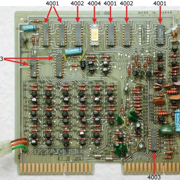
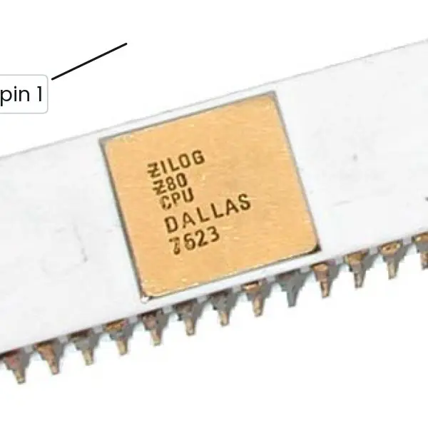
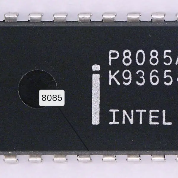
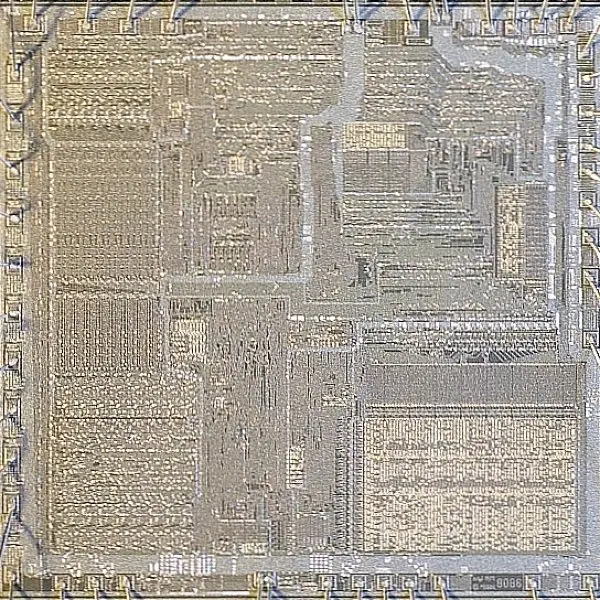
A processor is easy to picture once you have seen the real silicon and watched the signals move. The plate shows four chips from the history of this unit.
The figures then show the three buses, how one set of eight pins carries both an address and a data byte, the timing of a real 13 T-state instruction drawn to scale, and the flag register filled in for the worked example of Section 1.4.


1.9.1 Eight applications of microprocessors
- Personal computers and laptops. The CPU of every computer is a microprocessor; the Intel 4004 of the plate started a line that led to the Core and Ryzen chips of today. It fetches and executes billions of instructions a second for browsing, office work and programming. A student in a Kathmandu cyber cafe or a college lab uses one every day.
- Mobile phones. A phone's system-on-chip puts several ARM processor cores, a graphics unit and a modem on one die. These cores run Android, the camera, the keyboard and apps such as eSewa, Khalti and the Nagarik App. Their low power use lets a battery last a day.
- Banking and ATMs. An ATM contains a microprocessor that reads the card, checks the PIN, drives the cash dispenser and talks to the bank network. Fonepay terminals and bank POS machines work the same way. The processor must follow the same steps exactly every time, which is why a fixed program in ROM is used.
- Embedded control in home appliances. Washing machines, microwave ovens, rice cookers and air conditioners use a small microcontroller to read sensors and switch heaters or motors. The program is stored in ROM and runs from the moment the power is switched on. Such chips are cheap, often 8-bit, and need no operating system.
- Automobiles. A modern car holds dozens of microprocessors: engine control, anti-lock brakes, airbags and the dashboard. A Nepali bus or motorbike with a fuel-injection engine uses an engine control unit that measures air and speed and decides the fuel amount in milliseconds. Real-time response matters more than raw speed here.
- Medical equipment. Digital thermometers, blood-pressure meters, ECG machines and pulse oximeters use microprocessors to convert sensor signals into numbers. District hospitals and health posts rely on such devices for quick measurement. The processor also checks its own readings and shows an alarm when a value is unsafe.
- Industrial control and power systems. Programmable controllers and smart meters in factories, hydropower stations and the Nepal Electricity Authority use microprocessors to read voltage, count units and switch loads. They log data and send it to a control room. A fault can be seen and handled in seconds instead of hours.
- Education and training kits. The 8085 and 8086 trainer kits in college laboratories let a BCA student type hex opcodes, run them and see registers change. Arduino and Raspberry Pi boards play the same role for modern projects. Learning on a small processor makes bigger CPUs, caches and pipelines easier to understand.
Formula and fact sheet
- Address lines n → 2ⁿ locations: 16 lines = 64 KB, 20 lines = 1 MB.
- T = 1/f; at 3 MHz T = 0.333 µs. Execution time = (total T-states) × T.
- Opcode fetch = 4 T (6 T for PUSH/CALL/RST); memory/I/O read or write = 3 T.
- Flags: S (D7), Z (D6), AC (D4), P (D2), CY (D0). MOV/MVI/LDA/STA/jumps change no flags.
- Interrupt priority: TRAP > RST 7.5 > RST 6.5 > RST 5.5 > INTR. Vectors 0024H, 003CH, 0034H, 002CH.
- 8086 physical address = segment × 16 + offset.
Chapter summary
- A microprocessor is a CPU on a chip; a system joins CPU, memory and I/O with address, data and control buses.
- The 8085 has an accumulator, six general registers (pairs BC, DE, HL; M = byte at HL), PC, SP and five flags S, Z, AC, P, CY.
- AD0–AD7 are multiplexed; ALE and a latch separate the low address byte from the data.
- An instruction cycle consists of machine cycles (opcode fetch plus reads/writes), each of 3–6 T-states.
- Five hardware interrupts with fixed priority and eight software RSTs.
- The 8086 adds a wider bus, a prefetch queue (BIU/EU), segmentation and hardware multiply/divide.
Practice
- Define microprocessor, microcomputer and microcontroller.
- Name the three buses of a microprocessor system, their direction and the 8085 width of each.
- Why are AD0–AD7 multiplexed? Describe the role of ALE and the 74LS373.
- List the five flags of the 8085 and say when each is set.
- Find the flags after 7FH + 01H and after 80H + 80H.
- Differentiate between T-state, machine cycle and instruction cycle.
- How many T-states and machine cycles does
LDA 2050Hneed? Show each cycle. - Compute the time taken by
MVI A,05H ; ADD B ; STA 3000H ; HLTon a 3 MHz 8085. - List the 8085 interrupts in order of priority with their vector addresses.
- Calculate the 8086 physical address for CS = 1A00H, IP = 0250H, and state two advantages of the 8086 over the 8085.
Answers and worked solutions
1. A microprocessor is a CPU on one chip; a microcomputer is a microprocessor with memory and I/O; a microcontroller has CPU, memory and I/O on a single chip.
2. Address (one-way, 16 lines), data (two-way, 8 lines), control (several lines, mixed direction).
3. To fit in 40 pins. ALE goes high at T1, the latch captures AD0–AD7 as A0–A7, then the pins carry data while the latch keeps the address stable.
4. S (result negative), Z (result zero), AC (carry from bit 3), P (even parity), CY (carry/borrow).
5. 7FH + 01H = 80H: S = 1, Z = 0, CY = 0, AC = 1 (F + 1 carries), P = 0. 80H + 80H = 100H → result 00H: S = 0, Z = 1, CY = 1, AC = 0, P = 1.
6. T-state = one clock period; machine cycle = one bus operation (3–6 T); instruction cycle = all machine cycles of one instruction.
7. 13 T, 4 machine cycles: opcode fetch (4), memory read low address byte (3), memory read high address byte (3), memory read data (3).
8. 7 + 4 + 13 + 5 = 29 T × 0.333 µs = 9.67 µs.
9. TRAP (0024H) > RST 7.5 (003CH) > RST 6.5 (0034H) > RST 5.5 (002CH) > INTR (8n via RST n).
10. 1A00H × 16 = 1A000H; + 0250H = 1A250H. Advantages: 1 MB addressing; 16-bit data bus/prefetch queue; hardware multiply/divide.
Model answers for Unit 1
Q1. Name and explain the three buses of a microprocessor system. Show how the 8085 reads one byte from memory. (5 marks)
A bus is a group of wires shared by the CPU, memory and I/O devices (Fig. 1.1). The microprocessor system has three of them.
- Address bus. It is one-way, from the CPU to memory and I/O. The 8085 has 16 address lines, so it can select 2^{16} = 65,536 locations, which is 64 KB. The address says where the transfer happens.
- Data bus. It is two-way. The 8085 has 8 data lines, so one byte moves at a time. It carries instructions and data, and its width equals the word length.
- Control bus. It is a mix of single lines such as RD', WR', IO/M', ALE and READY. They say what kind of transfer it is (read or write, memory or I/O) and keep the timing.
Reading a byte from 2050H. (a) The CPU places 2050H on the address bus (A15-A8 = 20H, AD7-AD0 = 50H). (b) It sets IO/M' low (memory) and then makes RD' low, the memory-read signal.
(c) The memory chip that decodes 2050H puts its byte on the data bus. (d) The CPU latches the byte into a register and raises RD'. A write is the same, except that the CPU drives the data bus and uses WR'.
The CPU is the bus master and memory is a slave, so two devices never drive the data bus at the same time.
Q2. Why are the lines AD0-AD7 of the 8085 multiplexed? Explain the role of ALE and the 74LS373 latch. (5 marks)
The 8085 is packed in a 40-pin package. A full design would need 16 address pins and 8 data pins, but the CPU also needs pins for power, clock, interrupts, DMA, serial I/O and control.
To save pins the designers used the same eight pins, AD0-AD7, for two jobs at different times (Fig. 1.2). This is called multiplexing.
- In T1 of every machine cycle the pins carry the low-order address byte A0-A7. At that moment the CPU raises ALE (Address Latch Enable) for one clock.
- The external 74LS373 is a transparent octal latch. While ALE is high it is open and copies its inputs to its outputs. When ALE falls, the latch freezes and keeps A0-A7 steady.
- From T2 onward the same pins carry the data byte D0-D7. The latch ignores them because ALE is low, so the memory still sees a stable address.
The high address byte A8-A15 comes straight from separate pins. Together with the latch outputs it forms the full 16-bit address.
Without ALE and the latch, the address would vanish as soon as data appeared on the pins, and the memory could not select a location. The cost of multiplexing is one extra chip and a small delay; the gain is a smaller, cheaper package.
Q3. Describe the architecture of the Intel 8085 microprocessor with a block explanation of its registers, ALU, flags and control unit. Compare it with the 8086. (10 marks)
Introduction. The Intel 8085 (1976) is an 8-bit microprocessor in a 40-pin package that works from a single +5 V supply and an on-chip clock generator. It has an 8-bit data bus, a 16-bit address bus (64 KB memory) and 256 I/O ports.
Its internal blocks are joined by an internal data bus (Section 1.3; chip photo in Plate 1.1).
Functional blocks.
- ALU. It adds, subtracts, ANDs, ORs, XORs, compares, rotates, increments and decrements. One input is the accumulator and the other is a temporary register.
- Accumulator. An 8-bit register that holds one operand and receives the result.
- Registers. B, C, D, E, H and L are 8-bit and can be paired as BC, DE and HL. HL also acts as the memory pointer M. W and Z are internal temporary registers that the programmer cannot use.
- Program counter (16-bit) holds the address of the next instruction and is incremented after each fetch. The stack pointer (16-bit) points to the top of the stack in RAM.
- Flag register. Five flags describe the result: S, Z, AC, P, CY. Conditional jumps test them (Fig. 1.4).
- Instruction register and decoder. The opcode is held here and decoded.
- Timing and control unit. It produces RD', WR', IO/M', ALE and the other signals in step with the clock. A 6 MHz crystal gives a 3 MHz internal clock.
- Interrupt and serial control. It handles TRAP, RST 7.5, 6.5, 5.5 and INTR, and the serial pins SID and SOD.
Execution. Every instruction is an instruction cycle made of machine cycles, each of 3-6 T-states; for example LDA 2050H takes 13 T-states (Fig. 1.3).
Comparison of 8085 and 8086.
| Point | 8085 | 8086 |
|---|---|---|
| Data bus | 8-bit | 16-bit |
| Address bus / memory | 16-bit, 64 KB | 20-bit, 1 MB (segmented) |
| Registers | A, B-L, 16-bit PC, SP | AX, BX, CX, DX, SI, DI, BP, SP, segment registers |
| Pre-fetching | none | 6-byte queue (BIU + EU work in parallel) |
| Multiply / divide | no instruction | hardware MUL and DIV |
| Clock | 3-5 MHz | 5-10 MHz |
| Address/data pins | AD0-AD7 multiplexed | AD0-AD15 multiplexed |
Conclusion. The 8085 is simple enough to understand completely: registers feed the ALU, flags record the outcome, and the timing unit sequences every bus cycle.
The 8086 keeps the same ideas but adds a wider bus, a prefetch queue and segmentation, which is why it was the base of the PC family.
Q4. Draw the timing of LDA 2050H and find its execution time on a 3 MHz 8085. (5 marks)
LDA 2050H is a three-byte instruction (opcode 3AH, then the low byte 50H and the high byte 20H) that loads the accumulator from memory location 2050H. Suppose it is stored at 2000H. It needs four machine cycles (Fig. 1.3):
| Machine cycle | Job | T-states |
|---|---|---|
| M1 opcode fetch | read 3AH from 2000H; decode; PC incremented | 4 |
| M2 memory read | read the low address byte 50H from 2001H | 3 |
| M3 memory read | read the high address byte 20H from 2002H | 3 |
| M4 memory read | read the data byte from 2050H into A | 3 |
The total is 4 + 3 + 3 + 3 = 13 T-states. A 6 MHz crystal gives a 3 MHz clock, so one T-state is 1 / 3 MHz = 0.333 microsecond. The execution time is 13 x 0.333 = 4.33 microseconds.
The opcode-fetch cycle is longer by one T-state because the CPU decodes the opcode during T4. A faster 5 MHz 8085A-2 would need only 13 x 0.2 = 2.6 microseconds for the same instruction.