Unit 3 · 29 min read
Basic Computer Architecture
What the syllabus asks for 7
- Architecture, organisation and a little history
- The stored-program organisation
- The registers of the basic computer
- The instruction set of the basic computer
- Timing and control
- The instruction cycle
- Seeing the ideas: stored programs, buses, instruction cycle and interrupts
The 8085 shows a real chip; this unit shows the idea of a computer with every detail visible. We use the textbook basic computer (Mano): 16-bit words, 4096 words of memory, a handful of registers, seven memory-reference instructions.
It is small enough to trace by hand, yet it contains the stored-program principle, the instruction cycle and the interrupt mechanism that real machines use.
- Computer architecture versus computer organisation; a short history; the memory hierarchy.
- The stored-program organisation, instruction codes, direct and indirect addressing.
- The registers and the common bus of the basic computer.
- The instruction set (memory-reference, register-reference, I/O) and the timing and control signals.
- The instruction cycle: fetch, decode, indirect, execute, and the interrupt cycle.
3.1 Architecture, organisation and a little history
- Computer architecture = the attributes visible to the programmer: instruction set, data types, addressing modes, registers, I/O model. (What does the machine do?)
- Computer organisation = how that is realised in hardware: control signals, interfaces, memory technology, bus widths. (How is it built?)
The same architecture (say x86) is implemented by many organisations over the years.
| Generation | Period | Technology | Landmark |
|---|---|---|---|
| 0 | 1830s–40s | mechanical/relay | Babbage's Analytical Engine; Zuse Z3 |
| 1 | 1940s–50s | vacuum tubes | ENIAC (1946), von Neumann's stored-program EDVAC/IAS design |
| 2 | 1950s–60s | transistors | IBM 7090, early minicomputers |
| 3 | 1960s–70s | integrated circuits | IBM System/360 (architecture as a family), PDP-8 |
| 4 | 1970s– | microprocessors, VLSI | Intel 4004 (1971), 8085, 8086, PCs |
| 5+ | 1990s– | multi-core, GPUs, mobile SoCs | Pentium, ARM, multicore, ML accelerators |
Von Neumann and Harvard
The von Neumann architecture keeps instructions and data in the same memory and uses one bus, so the CPU can fetch only one thing at a time — the von Neumann bottleneck.
The Harvard architecture has separate instruction and data memories and buses, allowing both to be accessed at once (used in DSPs, microcontrollers, and, in effect, in the split L1 caches of modern CPUs).
Overview of computer organisation and the memory hierarchy
A computer has an input unit, an output unit, a memory, a control unit and an ALU (the last two make the CPU). No memory is simultaneously large, fast and cheap, so a hierarchy is built:
| Level | Typical size | Typical access time | Managed by |
|---|---|---|---|
| Registers | < 1 KB | < 1 ns | compiler |
| Cache (L1/L2/L3) | KB – MB | 1–20 ns | hardware |
| Main memory (RAM) | GB | 50–100 ns | operating system |
| Secondary store (SSD/HDD) | hundreds of GB – TB | 0.1 ms (SSD), ~10 ms (HDD) | OS |
Going down, capacity and latency rise and cost per bit falls. It works because of the principle of locality: programs reuse data (temporal locality) and use nearby data (spatial locality). Unit 6 treats cache and virtual memory in detail.
3.2 The stored-program organisation
In a stored-program computer the program is just data in memory: instructions are fetched, decoded and executed in sequence, and a program can be replaced by loading different words. The basic computer has:
- Memory: 4096 words × 16 bits (a 12-bit address).
- Registers (below) and a 16-bit ALU.
- Control unit generating timing and control signals.
Instruction format
Each 16-bit instruction is split into an addressing-mode bit I, a 3-bit opcode and a 12-bit address field:
 15  14 13 12  11                 0
┌───┬────────┬─────────────────────┐
│ I │ opcode │       address       │
└───┴────────┴─────────────────────┘
- I = 0: direct addressing — the address field is the operand's address.
- I = 1: indirect addressing — the address field points to a memory word that holds the operand's address. Indirect addressing lets a program use pointers and tables, at the cost of an extra memory access.
- Opcode = 111 is special: with I = 0 the remaining 12 bits select a register-reference instruction; with I = 1 an input/output instruction. Opcodes 000–110 are the seven memory-reference instructions.
Memory: M[300] = 1350 and M[1350] = 77.
ADD 300 (I = 0): the operand is M[300] = 1350.
ADD I 300 (I = 1): M[300] = 1350 is an address; the operand is M[1350] = 77.
So the same address field gives two different operands depending on I.
3.3 The registers of the basic computer
| Register | Bits | Function |
|---|---|---|
| AR address register | 12 | holds the address of the memory word being accessed |
| PC program counter | 12 | address of the next instruction |
| DR data register | 16 | holds the memory operand |
| AC accumulator | 16 | general working register; the ALU result lands here |
| IR instruction register | 16 | holds the instruction being executed |
| TR temporary register | 16 | temporary data (used in the interrupt cycle) |
| INPR input register | 8 | one character from the input device |
| OUTR output register | 8 | one character for the output device |
| SC sequence counter | 4 | counts the timing steps T0, T1, T2… |
| E | 1 | extended AC bit — carry-out and rotate extension |
| FGI, FGO | 1 each | input/output flags (ready) |
| IEN, R | 1 each | interrupt-enable flip-flop; interrupt-request flip-flop |
The common bus system
Seven registers must exchange data; wiring each pair separately would be unmanageable. A common bus — 16 lines — is shared.
Three select bits S2 S1 S0 control a multiplexer that picks which register drives the bus (000 none, 001 AR, 010 PC, 011 DR, 100 AC, 101 IR, 110 TR, 111 memory).
Each register has a load (LD), increment (INR) and clear (CLR) input; the destination register is the one whose LD is enabled. Memory has read and write controls.
The AC input is not the bus but the ALU output (which adds AC and DR, and offers AND, complement, shift), and AC also drives the bus. Only one source may drive the bus at a time; many destinations may load from it at the same time.
         ┌── memory (read/write) ──┐
 AR PC DR AC IR TR  ──►  [ mux S2 S1 S0 ]  ──►  common bus (16)  ──►  every register's input
                                                       ▲
                                              ALU (AC, DR, INPR) ──► AC
3.4 The instruction set of the basic computer
Memory-reference instructions (opcode 000–110)
| Symbol | Opcode (I = 0 / I = 1) | Operation (register-transfer) |
|---|---|---|
| AND | 0xxx / 8xxx | AC ← AC ∧ M[AR] |
| ADD | 1xxx / 9xxx | AC ← AC + M[AR], E ← carry-out |
| LDA | 2xxx / Axxx | AC ← M[AR] |
| STA | 3xxx / Bxxx | M[AR] ← AC |
| BUN | 4xxx / Cxxx | branch unconditionally: PC ← AR |
| BSA | 5xxx / Dxxx | branch and save return address: M[AR] ← PC, PC ← AR + 1 |
| ISZ | 6xxx / Exxx | M[AR] ← M[AR] + 1; if it becomes 0, PC ← PC + 1 (skip) |
Register-reference instructions (7xxx, I = 0, one bit set)
| Symbol | Code | Operation |
|---|---|---|
| CLA | 7800 | AC ← 0 |
| CLE | 7400 | E ← 0 |
| CMA | 7200 | AC ← AC′ |
| CME | 7100 | E ← E′ |
| CIR | 7080 | circulate right AC and E |
| CIL | 7040 | circulate left AC and E |
| INC | 7020 | AC ← AC + 1 |
| SPA | 7010 | skip next if AC positive |
| SNA | 7008 | skip next if AC negative |
| SZA | 7004 | skip next if AC zero |
| SZE | 7002 | skip next if E zero |
| HLT | 7001 | halt |
Input–output instructions (Fxxx, I = 1)
| Symbol | Code | Operation |
|---|---|---|
| INP | F800 | AC(0–7) ← INPR, FGI ← 0 |
| OUT | F400 | OUTR ← AC(0–7), FGO ← 0 |
| SKI | F200 | skip next if FGI = 1 |
| SKO | F100 | skip next if FGO = 1 |
| ION | F080 | IEN ← 1 |
| IOF | F040 | IEN ← 0 |
The instruction set is complete in the sense that it supports arithmetic, logic, data movement, program control and I/O — subtraction is done by complement and increment (CMA, INC, ADD), shifts by CIR/CIL, comparisons by subtraction and SPA/SNA/SZA.
Add the numbers in locations 100 and 101 and store the result in 102 (program at 000):
000  LDA 100     ; AC ← M[100]            (2100)
001  ADD 101     ; AC ← AC + M[101]       (1101)
002  STA 102     ; M[102] ← AC            (3102)
003  HLT         ;                        (7001)
With M[100] = 0005 and M[101] = 0003: after LDA, AC = 5; after ADD, AC = 8; STA writes 8 to 102. Subtraction M[100] − M[101]: LDA 101, CMA, INC (AC = −M[101]), ADD 100, STA 102.
For 5 − 3: AC = 3 → CMA FFFC → INC FFFD (= −3) → ADD 5 → 0002 with E = 1 (the discarded carry).
3.5 Timing and control
The control unit uses a sequence counter SC feeding a 4-to-16 decoder that produces timing signals T0 … T15. SC is incremented every clock; at the end of an instruction it is cleared (SC ← 0) so the next fetch starts at T0.
Another decoder (3-to-8) decodes the opcode bits 12–14 of IR into D0 … D7; the I bit is IR(15).
Control signals are Boolean functions of Tᵢ, Dⱼ, I, the flags and the flip-flop R. For example, the signal that loads AR from the PC is R′T0, and the signal that adds DR to AC is D1T5.
(The next unit compares building these functions in gates — hardwired control — with storing them in a memory — microprogrammed control.)
3.6 The instruction cycle
Every instruction goes through repeating phases: 1. fetch the instruction from memory; 2. decode the opcode; 3. read the effective address from memory if the instruction is indirect; 4. execute; then go back to step 1 for the next instruction (unless R = 1: the interrupt cycle).
Fetch and decode (T0–T2, when R = 0)
R′T0 :  AR ← PC
R′T1 :  IR ← M[AR],  PC ← PC + 1
R′T2 :  D0 … D7 ← decode IR(12–14),  AR ← IR(0–11),  I ← IR(15)
The decision after T2
D7′ I  T3 :  AR ← M[AR]              (memory-reference, indirect)
D7′ I′ T3 :  (nothing)               (memory-reference, direct)
D7  I′ T3 :  execute register-reference
D7  I  T3 :  execute input-output
Memory-reference instructions proceed from T4:
AND  D0T4 :  DR ← M[AR]                    D0T5 :  AC ← AC ∧ DR, SC ← 0
ADD  D1T4 :  DR ← M[AR]                    D1T5 :  AC ← AC + DR, E ← Cout, SC ← 0
LDA  D2T4 :  DR ← M[AR]                    D2T5 :  AC ← DR, SC ← 0
STA  D3T4 :  M[AR] ← AC, SC ← 0
BUN  D4T4 :  PC ← AR, SC ← 0
BSA  D5T4 :  M[AR] ← PC, AR ← AR + 1       D5T5 :  PC ← AR, SC ← 0
ISZ  D6T4 :  DR ← M[AR]
     D6T5 :  DR ← DR + 1
     D6T6 :  M[AR] ← DR, if (DR = 0) then (PC ← PC + 1), SC ← 0
Register-reference instructions execute in T3 only, e.g. D7I′T3·B11 : AC ← 0, SC ← 0 for CLA (the bit B11 is the instruction's IR(11) bit).
Let PC = 010, M[010] = 1100 (ADD, I = 0, address 100), M[100] = 0003, AC = 0005.
- T0: AR ← 010.
- T1: IR ← 1100, PC ← 011.
- T2: D1 = 1 (opcode 001), AR ← 100, I = 0.
- T3: nothing (direct).
- T4: DR ← M[100] = 0003.
- T5: AC ← 0005 + 0003 = 0008, E ← 0, SC ← 0. Six clock pulses (T0–T5); the next instruction starts with PC = 011. With an indirect ADD the otherwise idle T3 is used to load AR ← M[AR] (the pointer), so the instruction still takes six pulses — the basic computer's direct memory-reference instructions simply waste T3 to keep the timing uniform.
BSA 200 at address 010: T4 M[200] ← PC = 011 (the return address), AR ← 201; T5 PC ← 201. The subroutine runs from 201; to return, it executes BUN 200 I (indirect): AR ← M[200] = 011, PC ← 011.
This is the basic computer's only subroutine mechanism — note that it stores the return address in the subroutine's own first word, so it cannot be used recursively.
The interrupt cycle
The flip-flop R is set (an interrupt is taken) when IEN = 1 and either FGI or FGO = 1 at the end of an instruction. When R = 1 the fetch phase is replaced by:
RT0 :  AR ← 0,  TR ← PC
RT1 :  M[AR] ← TR,  PC ← 0
RT2 :  PC ← PC + 1,  IEN ← 0,  R ← 0,  SC ← 0
So the return address is saved in location 0 and execution continues at location 1, where a BUN jumps to the service routine, which must find which device raised the flag (by testing FGI, FGO), service it, re-enable interrupts with ION and return with an indirect BUN 0 I.
IEN is cleared automatically so the routine is not itself interrupted before it finishes.
3.7 Seeing the ideas: stored programs, buses, instruction cycle and interrupts
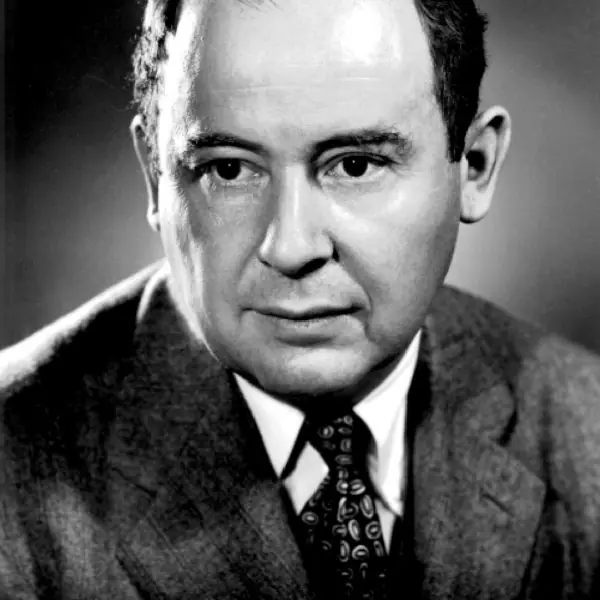
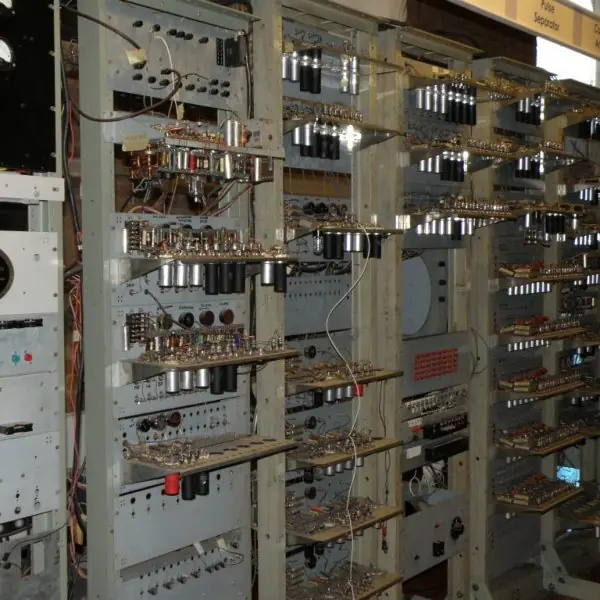
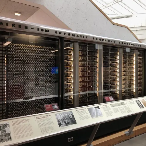
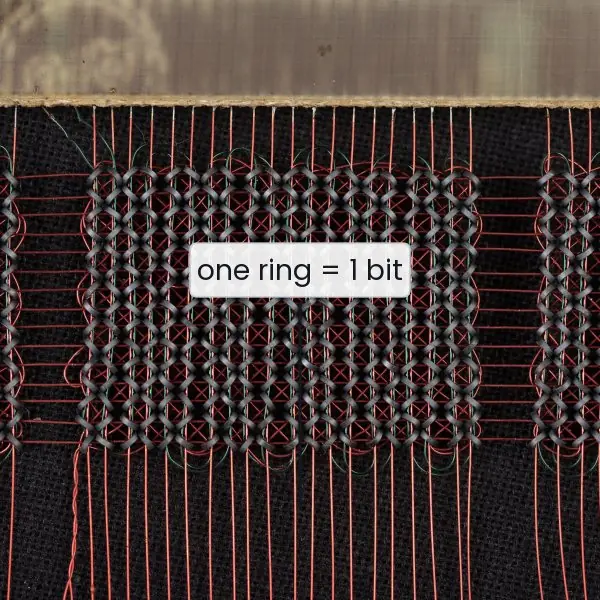
The basic computer is a paper design, but its ideas come from real machines. The plate shows the people and machines behind the stored-program concept and the core memory it ran on.
The figures compare the two architectures, show how a direct and an indirect address reach different operands, follow a real three-instruction program clock by clock, and show what the interrupt cycle does to memory.
The traces were produced by a register-transfer simulator of the basic computer written for this book.


3.7.1 Eight advantages of the stored-program concept
- One machine, many jobs. Because the program is stored in memory, the same hardware can run a payroll, a game or a result-processing job just by loading a different program. Before the Manchester Baby, changing the job meant rewiring plugboards. A college computer lab uses the same PC for programming, accounting and web browsing.
- Fast changes. To correct or improve a program, only the words in memory change, which takes seconds. A mistake in the Tribhuvan University results program can be fixed and re-run the same day. No hardware needs to be touched.
- Programs are data. Instructions are stored as numbers like any other data, so a program can be loaded, copied, saved and even modified by another program. This is how compilers, loaders and operating systems work. It also explains how a virus can change code in memory.
- Speed of execution. Instructions are fetched at electronic speed from memory, not read from slow tape or switches. The Harvard Mark I needed a motor-driven tape; a modern CPU fetches billions of instructions each second. This is the basis of the high speed of every present-day computer.
- Branching and loops. Since the program counter is just a register that can be changed, instructions such as BUN and ISZ let the program repeat or choose a path. The loop of 5 x 5 in the model answers takes only six instructions. Without this, programs would be as long as the work they do.
- Subroutines and reuse. A routine written once can be called from many places with BSA (the return address is saved in memory, as Fig. 3.4 shows for interrupts). An ATM, a ConnectIPS page and a Nagarik App form all reuse the same library routines. Reuse saves memory and reduces errors.
- Simple hardware design. Because instructions and data share one memory and one bus (Fig. 3.1), the hardware has fewer parts and is cheaper. The basic computer needs only a handful of registers and a common bus. This simplicity is why the model suits teaching and early microprocessors like the 8085.
- A universal standard. Almost every general-purpose computer, from a Raspberry Pi to a bank server, follows this model, so programs and ideas move easily between machines. Textbooks, compilers and operating systems depend on it. Learning the basic computer therefore helps a student with every later machine.
Formula and fact sheet
- Basic computer: 4096 × 16 memory; AR, PC 12 bits; DR, AC, IR, TR 16 bits; INPR, OUTR 8 bits; SC 4 bits.
- Instruction = I (1) + opcode (3) + address (12). Opcode 111 → register-reference (I = 0) or I/O (I = 1).
- Fetch: T0 AR ← PC; T1 IR ← M[AR], PC ← PC + 1; T2 decode, AR ← IR(0–11).
- ADD: DR ← M[AR] (T4), AC ← AC + DR (T5). Direct and indirect both take T0–T5 (indirect uses T3 for AR ← M[AR]); ISZ takes T0–T6.
- Interrupt: R = 1 → save PC in M[0], PC ← 1, IEN ← 0.
- Subtraction = CMA, INC, ADD. Two's complement of x is x′ + 1.
Chapter summary
- Architecture is what the programmer sees; organisation is how it is built. The von Neumann machine stores program and data together; the memory hierarchy exploits locality.
- The basic computer has AR, PC, DR, AC, IR, TR, INPR, OUTR, a 16-bit common bus and a ripple of load/increment/clear controls.
- Instructions are I + 3-bit opcode + 12-bit address; seven memory-reference, twelve register-reference and six I/O instructions.
- The control unit derives timing T0–T15 from a sequence counter and D0–D7 from the opcode.
- Fetch takes T0–T2, indirect addressing adds a read, and each instruction clears SC when done; an interrupt replaces fetch with the three-step interrupt cycle.
Practice
- Distinguish between computer architecture and computer organisation.
- Draw and explain the instruction format of the basic computer, including direct and indirect addressing.
- List the registers of the basic computer with their sizes and purposes.
- How does the common bus system work? Why is it used?
- Write a basic-computer program to compute M[200] + M[201] − M[202] and store it in 203.
- Write the register transfers (with timing signals) for the fetch phase and for
LDA. - Trace the execution of
BSA 300located at 050. How does it return? - How many clock cycles does a direct
ISZtake, and what does it do when the word becomes zero? - Explain the interrupt cycle of the basic computer and the role of IEN and R.
- What is the memory hierarchy? State the principle that makes it work.
Answers and worked solutions
1. Architecture = programmer-visible features (instruction set, registers, addressing); organisation = hardware realisation (control signals, interfaces, memory technology).
2. 16 bits: bit 15 = I, bits 12–14 = opcode, bits 0–11 = address. I = 0 → the address field is the operand address; I = 1 → it is the address of the address.
3. AR 12 (address), PC 12 (next instruction), DR 16 (memory operand), AC 16 (accumulator), IR 16 (instruction), TR 16 (temporary), INPR 8, OUTR 8, SC 4 (timing).
4. A 16-line bus shared by all registers; selection bits S2S1S0 choose the one source; a destination loads when its LD is on. It cuts the number of wires from ~n² to n.
5. LDA 200 ; ADD 201 ; STA 204 ; LDA 202 ; CMA ; INC ; ADD 204 ; STA 203 ; HLT (204 is a scratch word). Check with 9, 4, 3: 9 + 4 = 13, −3 = FFFD, 13 + (−3) = 10.
6. Fetch: R′T0 AR ← PC; R′T1 IR ← M[AR], PC ← PC + 1; R′T2 decode, AR ← IR(0–11), I ← IR(15). LDA: D2T4 DR ← M[AR]; D2T5 AC ← DR, SC ← 0.
7. T4: M[300] ← 051 (PC after fetch), AR ← 301; T5: PC ← 301. Return with BUN 300 I: AR ← M[300] = 051 ⇒ PC ← 051.
8. Direct ISZ: T0–T2 fetch, T3 idle, T4 read, T5 increment, T6 write-back and test: 7 cycles. If DR becomes 0, PC ← PC + 1, i.e. the next instruction is skipped.
9. When IEN = 1 and a device flag (FGI or FGO) is set, R becomes 1. The next cycle saves PC in M[0], sets PC = 1, clears IEN and R; the program at location 1 branches to the service routine.
10. A layered structure from registers to cache, RAM and disk, balancing cost, capacity and speed; the principle of locality of reference.
Model answers for Unit 3
Q1. Differentiate between the von Neumann and Harvard architectures. (5 marks)
The von Neumann architecture keeps instructions and data in one memory, joined to the CPU by one set of buses. The Harvard architecture uses separate memories and separate buses for instructions and data (Fig. 3.1).
The two names come from the machines of Plate 3.1: von Neumann described the stored-program computer in 1945, and the Harvard Mark I (1944) read instructions from a paper tape and kept data in counters.
| Point | Von Neumann | Harvard |
|---|---|---|
| Memory | single, shared | separate instruction and data memory |
| Buses | one address and data path | two sets of buses |
| Fetch and data access | one at a time (bottleneck) | can overlap |
| Hardware cost | lower, simpler | higher, more pins and buses |
| Flexibility | programs can be treated as data, so loaders and compilers are easy | instruction memory is often read-only |
| Used in | PCs, laptops, the 8085 | DSP chips, many microcontrollers |
Modern practice. A modern CPU is a mix: main memory is shared (von Neumann), but the L1 cache is split into an instruction cache and a data cache (Harvard) so that fetch and data access can proceed together.
The single shared path to main memory is still called the von Neumann bottleneck.
Q2. Explain the instruction format of the basic computer. Differentiate direct and indirect addressing with an example. (5 marks)
The basic computer has 16-bit instructions with three fields (Fig. 3.2).
- I (bit 15) is the addressing-mode bit: 0 = direct, 1 = indirect.
- Opcode (bits 14-12) has 3 bits, so there are eight codes. Codes 000-110 are the seven memory-reference instructions (AND, ADD, LDA, STA, BUN, BSA, ISZ). Code 111 means register-reference (when I = 0) or input-output (when I = 1).
- Address (bits 11-0) has 12 bits, so memory has 2^{12} = 4096 words.
Direct addressing (I = 0): the address field is the operand's address. Indirect addressing (I = 1): the address field points to a word that contains the operand's address.
Example. Let M[300] = 1350 and M[1350] = 77. ADD 300 uses the operand M[300] = 1350. ADD I 300 reads M[300] = 1350 as an address and uses M[1350] = 77.
Indirect addressing needs one more memory read (done in the otherwise idle T3), but it makes pointers, tables and subroutine returns possible. The same field therefore gives two different operands depending on I.
Q3. Describe the registers of the basic computer and the common bus system. (10 marks)
Introduction. The basic computer (Mano) has 4096 words of 16 bits, a 16-bit ALU and a small set of registers that exchange data over a common bus. Its design is the standard example for the stored-program idea (Plate 3.1, Fig. 3.1).
Registers.
- AR (12 bits) holds the address of the memory word being read or written.
- PC (12 bits) holds the address of the next instruction and is incremented after each fetch.
- DR (16 bits) holds the operand read from memory.
- AC (16 bits) is the accumulator; the ALU result is placed here.
- IR (16 bits) holds the instruction being executed.
- TR (16 bits) is a temporary register, used in the interrupt cycle.
- INPR and OUTR (8 bits each) hold one input and one output character.
- SC (4 bits) counts the timing steps T0, T1, T2 and so on; it is cleared at the end of every instruction.
The single-bit registers are E (extension of AC; carry-out), I (indirect bit), R (interrupt request), IEN (interrupt enable) and the flags FGI and FGO.
Common bus. Wiring every register to every other would need far too many wires, so all the registers share one 16-line bus.
Three select lines S2 S1 S0 drive a multiplexer that chooses which source drives the bus: 001 AR, 010 PC, 011 DR, 100 AC, 101 IR, 110 TR, 111 memory.
Each destination register has a load (LD) input, and also INR (increment) and CLR (clear) where needed, so only the chosen register captures the bus value in a clock pulse.
The ALU takes AC and DR (and INPR) and writes its result to AC; AC can also drive the bus.
Example of a transfer. For AR <- PC the control sets S2S1S0 = 010 and enables LD of AR. For IR <- M[AR] it sets S2S1S0 = 111 (memory) and enables LD of IR.
Comparison with separate wiring. With seven registers, point-to-point wiring needs about 7 x 6 = 42 links of 16 bits; the common bus needs one set of 16 lines and a multiplexer.
Conclusion. The registers hold addresses, data, instructions and flags, and the common bus with select lines lets one register at a time send data.
The cost is that only one transfer can happen per clock pulse, which is why the control unit orders every step as T0, T1, T2 and so on.
Q4. Explain the instruction cycle of the basic computer. Trace a real program through it. (10 marks)
Introduction. Every instruction passes through four phases: fetch, decode, read the effective address (if indirect) and execute, then the cycle repeats. The control unit follows the timing signals T0, T1, T2 from the sequence counter SC (Fig. 3.3).
Fetch and decode (when R = 0):
R'T0 : AR <- PC
R'T1 : IR <- M[AR],  PC <- PC + 1
R'T2 : decode IR(12-14),  AR <- IR(0-11),  I <- IR(15)
After T2. If the opcode is 111 and I = 0, a register-reference instruction runs in T3. If it is 111 and I = 1, an input-output instruction runs in T3. For opcodes 000-110, T3 does AR <- M[AR] when I = 1 and nothing when I = 0; execution begins at T4.
Execute phases of the memory-reference instructions.
| Instruction | Steps | Pulses |
|---|---|---|
| AND | T4 DR <- M[AR]; T5 AC <- AC AND DR | 6 |
| ADD | T4 DR <- M[AR]; T5 AC <- AC + DR, E <- carry | 6 |
| LDA | T4 DR <- M[AR]; T5 AC <- DR | 6 |
| STA | T4 M[AR] <- AC | 5 |
| BUN | T4 PC <- AR | 5 |
| BSA | T4 M[AR] <- PC, AR <- AR + 1; T5 PC <- AR | 6 |
| ISZ | T4 DR <- M[AR]; T5 DR <- DR + 1; T6 M[AR] <- DR, skip if zero | 7 |
Every instruction ends with SC <- 0.
Real trace. The program LDA 006, ADD 007, STA 008, HLT (words 2006, 1007, 3008, 7001) with M[006] = 0053 and M[007] = 002F gave: after LDA, AC = 0053 and PC = 001; after ADD, AC = 0082 and PC = 002; after STA, M[008] = 0082.
The clock pulses were 6 + 6 + 5 + 4 = 21.
A second program with CLA, ADD 00A, ISZ 00B, BUN 001, STA 00C, HLT, with M[00A] = 0005 and a counter M[00B] = FFFB (minus 5), added 5 five times and stored 0019 (25), in 98 pulses, because ISZ skips the BUN when the counter reaches zero.
Conclusion. The instruction cycle is a fixed rhythm: T0-T2 fetch and decode, T3 for the mode, then execute. Because the rhythm is the same for every instruction, the control unit (Unit 4) only needs to decide which register transfers to enable at each step.
Q5. What is the interrupt cycle? Explain how the basic computer takes and returns from an interrupt. (5 marks)
An interrupt lets an I/O device call for attention without the CPU waiting. The basic computer sets the flip-flop R = 1 at the end of an instruction when IEN = 1 and either flag FGI or FGO is 1. With R = 1 the normal fetch is replaced by the interrupt cycle (Fig. 3.4):
RT0 : AR <- 0,  TR <- PC
RT1 : M[AR] <- TR,  PC <- 0
RT2 : PC <- PC + 1,  IEN <- 0,  R <- 0,  SC <- 0
So the return address is saved in location 0 and execution continues at location 1, where a BUN jumps to the service routine.
The routine checks FGI and FGO to find the device, serves it and then runs ION (set IEN) and BUN 0 I, which reloads PC from location 0, so the interrupted program resumes where it stopped.
IEN is cleared in RT2 so that a second interrupt cannot overwrite location 0 until the routine has finished. The cycle takes three pulses, and the program only sees a short pause.