Unit 7 · 35 min read
Memory Organisation
What the syllabus asks for 7
- The memory hierarchy
- Primary memory: RAM and ROM
- Secondary memory: the magnetic disk
- Cache memory
- Virtual memory
- Memory management hardware
- Seeing the ideas: memory chips, the hierarchy, cache mapping, paging and replacement
Processor speed has long outrun memory speed. The answer is a hierarchy of memories, each level small and fast near the CPU and large and slow far from it, managed so the whole behaves like a large, fast memory.
This unit covers the hierarchy, RAM and ROM chips and their address maps, secondary storage, cache memory (mapping, replacement, writes), virtual memory (paging, page replacement), segmentation and protection.
- The memory hierarchy and the locality principle.
- RAM and ROM chip types, chip-select decoding and memory address maps.
- Magnetic disk structure and access time.
- Cache memory: hit ratio, three mapping schemes, replacement, write policies, average access time.
- Virtual memory: pages, page tables, page faults, FIFO/LRU/optimal replacement (Belady's anomaly).
- Segmented page mapping and memory protection.
7.1 The memory hierarchy
| Level | Technology | Size | Access time | Cost per bit |
|---|---|---|---|---|
| Registers | flip-flops in the CPU | hundreds of bytes | < 1 ns | highest |
| L1 cache | SRAM on the CPU chip | 32–64 KB | 1 ns | |
| L2/L3 cache | SRAM | 256 KB – 32 MB | 3–20 ns | |
| Main memory | DRAM | GBs | 50–100 ns | |
| Secondary | SSD / magnetic disk | 100 GB – TBs | 0.1 ms / 10 ms | |
| Archive | tape, optical | very large | seconds | lowest |
Principle of locality makes this effective: temporal locality (recently used items are likely to be used again soon — loops) and spatial locality (items near a used one are likely to be used soon — sequential code, arrays).
The upper levels hold copies of the data most likely to be needed.
7.2 Primary memory: RAM and ROM
| Type | Meaning | Notes |
|---|---|---|
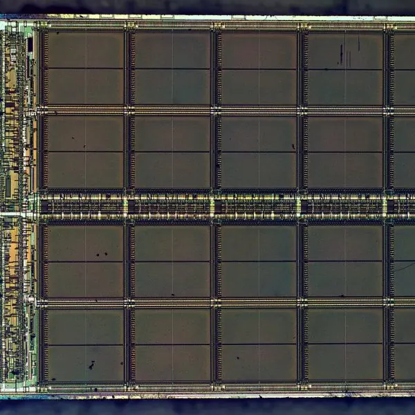
| SRAM | static RAM — flip-flop cells (6 transistors) | fast, no refresh, expensive, big per bit: cache |
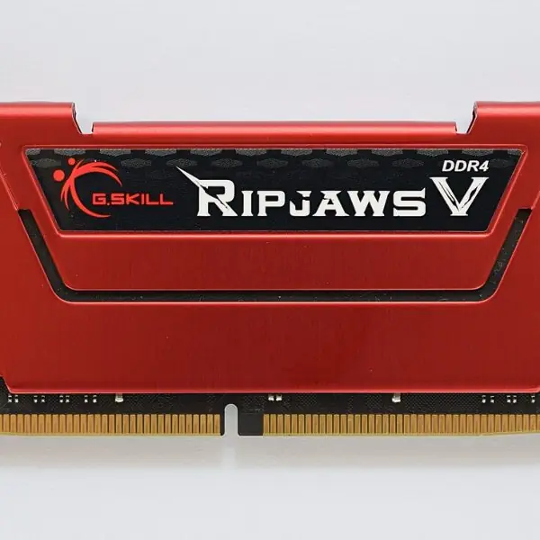
| DRAM | dynamic RAM — one transistor + capacitor | slower, needs periodic refresh (every few ms), cheap and dense: main memory (SDRAM, DDR) |
| ROM | read-only memory | holds boot program; non-volatile |
| PROM | programmable once by the user | |
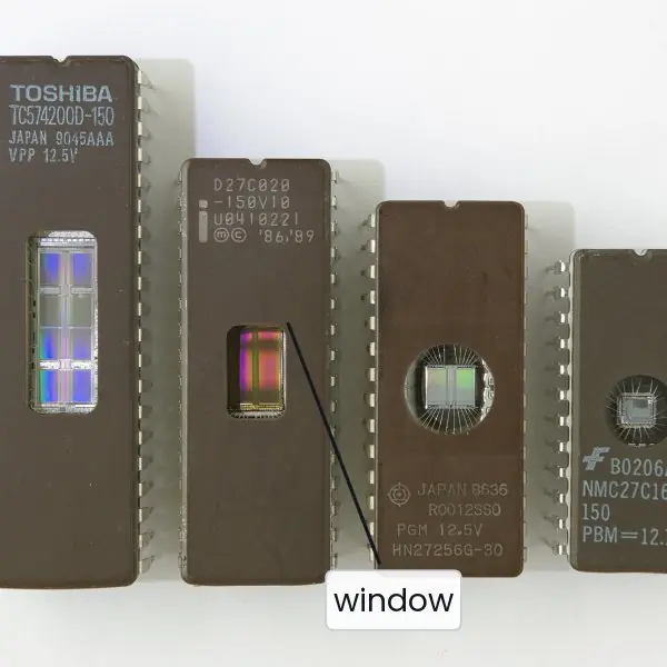
| EPROM | erasable by UV light, reprogrammable | quartz window |
| EEPROM | erasable electrically, byte by byte | settings storage |
| Flash | block-erasable EEPROM | SSDs, USB sticks, phone storage |
RAM is volatile (loses data at power-off); ROM is non-volatile.
Memory chip organisation and chip select
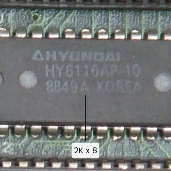
A 128 × 8 RAM chip has 7 address lines (2⁷ = 128), 8 data lines, chip-select (CS) inputs and read/write lines. When CS is not active the chip's data lines are high-impedance, so many chips can share the bus.
A 2K × 8 chip needs 11 address lines; a 64 KB space needs 16; building a 64 KB memory from 16K × 8 chips takes 4 chips and 2 address lines (A14, A15) to select among them via a 2-to-4 decoder.
The memory address map
A memory address map is a table listing which chip responds to which range of addresses.
Use four 128 × 8 RAM chips and one 512 × 8 ROM chip in a 10-bit address space (1024 bytes). Address line 10 (counting from 1; the 10th line, A9) selects RAM (0) or ROM (1).
Lines A8–A7 drive a 2-to-4 decoder choosing one of the four RAM chips; A6–A0 address within a RAM chip; A8–A0 address within the ROM.
| Component | A9 | A8 A7 | A6–A0 | Hex address range |
|---|---|---|---|---|
| RAM 1 | 0 | 00 | x | 0000 – 007F |
| RAM 2 | 0 | 01 | x | 0080 – 00FF |
| RAM 3 | 0 | 10 | x | 0100 – 017F |
| RAM 4 | 0 | 11 | x | 0180 – 01FF |
| ROM | 1 | xx | x | 0200 – 03FF |
(Range checks: four chips × 128 = 512 = 0x200, so RAM ends at 01FF and the 512-byte ROM occupies 0200–03FF — verified by the script.)
7.3 Secondary memory: the magnetic disk
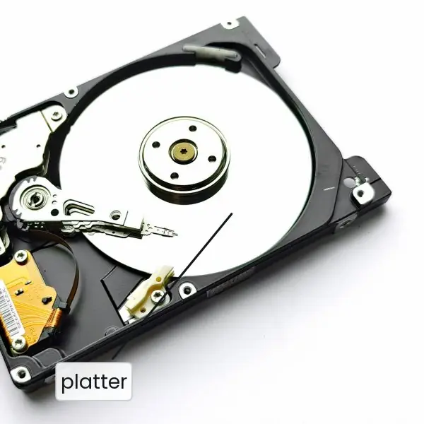
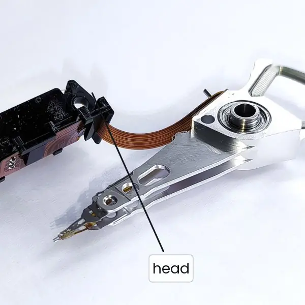
A hard disk has one or more platters coated with magnetic material, each surface served by a read/write head on an arm. Data are on concentric tracks; all tracks at the same arm position form a cylinder; each track is divided into sectors (commonly 512 bytes or 4 KB).
Capacity = surfaces × cylinders (tracks per surface) × sectors per track × bytes per sector.
Example 8 surfaces × 1000 cylinders × 63 sectors × 512 B = 258,048,000 bytes ≈ 258 MB.
Access time = seek time + rotational latency + transfer time.
- Seek time: moving the arm to the right cylinder (a few ms on average).
- Rotational latency: waiting for the sector to arrive under the head; on average half a revolution: at 7200 rpm, one revolution = 60/7200 s = 8.33 ms, so average latency = 4.17 ms.
- Transfer time: sector size ÷ transfer rate (microseconds for one sector).
Disks are about 10⁵–10⁶ times slower than DRAM, which is why caching and virtual memory exist. SSDs have no moving parts (no seek or rotational latency) and use flash memory.
7.4 Cache memory
A cache is a small, fast memory between the CPU and main memory that holds copies of recently used blocks.
- Hit: the word is in the cache. Miss: it is not; the whole block (line, e.g. 16 or 64 bytes) is fetched from main memory.
- Hit ratio h = hits ÷ total accesses; miss ratio = 1 − h.
- Average memory access time (AMAT) = h × t_cache + (1 − h) × (t_cache + t_memory) = t_cache + (1 − h) × t_memory.
Cache access 10 ns, main memory 100 ns, hit ratio 0.9. AMAT = 0.9 × 10 + 0.1 × (10 + 100) = 9 + 11 = 20 ns; without a cache each access costs 100 ns, so the cache gives a speed-up of 100/20 = 5.
A second case: cache 2 ns, memory 50 ns, h = 0.95: AMAT = 0.95 × 2 + 0.05 × 52 = 1.9 + 2.6 = 4.5 ns. (Both verified by script.)
Mapping functions — where does a memory block go?
Memory is divided into blocks the size of a cache line. A mapping function decides which cache line may hold a given block. Each cache line stores a tag identifying which block it currently holds, plus a valid bit.
| Mapping | Rule | Address split | Pros / cons |
|---|---|---|---|
| Direct | block j → line (j mod number of lines) | tag · index · offset | simplest, fastest; conflict misses if two active blocks share a line |
| Fully associative | a block may go in any line | tag · offset | no conflicts; needs comparing the tag against all lines (expensive) |
| Set associative (k-way) | block j → set (j mod number of sets); any of k lines in the set | tag · set · offset | the practical compromise (2-, 4-, 8-way) |
Main memory 64 KB (16-bit addresses), cache 1 KB, block (line) size 16 bytes. Offset = log₂16 = 4 bits. Number of lines = 1024/16 = 64 ⇒ index = 6 bits. Tag = 16 − 4 − 6 = 6 bits.
Address A3C7 = 1010 0011 1100 0111: tag = 101000 (28H), index = 111100 (3CH = line 60), offset = 0111 (7). The byte is in cache line 60 if its tag equals 28H.
For a 4-way set-associative cache of the same size: 64 lines ÷ 4 = 16 sets ⇒ index 4 bits, tag 8 bits.
Replacement policies (associative caches)
When a set is full, which line is evicted? LRU (least recently used — best in practice, needs bookkeeping), FIFO (oldest in), random, LFU (least frequently used). A direct-mapped cache needs no policy.
Write policies
| Policy | Operation | Notes |
|---|---|---|
| Write-through | write cache and main memory together | memory always up to date; slow unless a write buffer is used |
| Write-back | write the cache only; mark line dirty; write to memory when the line is evicted | far fewer memory writes; more complex (coherence in multi-core) |
| Write-allocate / no-write-allocate | on a write miss, load the block (or not) | usually write-back + write-allocate |
Cache coherence (several CPUs with private caches) is covered in Unit 8.
7.5 Virtual memory
Virtual memory gives each program the illusion of a very large, private, contiguous address space — bigger than physical memory — by keeping the program on disk and loading pages into RAM on demand.
- The CPU issues virtual (logical) addresses; the memory-management unit (MMU) translates them to physical addresses.
- Virtual space is divided into pages (typically 4 KB); physical memory into frames of the same size.
- A page table (per process) maps page numbers → frame numbers; each entry has a valid/present bit and protection bits.
virtual address = [ page number | offset ] ──► page table ──► [ frame number | offset ] = physical address
32-bit virtual address, 4 KB pages: offset = 12 bits, page number = 20 bits ⇒ 2²⁰ = 1,048,576 page-table entries; with 4-byte entries the page table is 4 MB per process (hence multi-level page tables).
Virtual address 0x00003A7C: page = 3, offset = A7C. If page-table[3] = frame 0x1B, the physical address = 0x1B·1000 + A7C = 0x0001BA7C.
Page fault and demand paging
If the valid bit is 0 the access causes a page fault (a trap): the OS finds a free frame (or evicts a page), reads the page from disk, updates the page table and restarts the instruction.
A page fault costs milliseconds, so the page-fault rate must be tiny: effective access time ≈ (1 − p) × t_mem + p × t_fault.
A TLB (translation lookaside buffer, a small cache of page-table entries) avoids the extra memory access for the page table on most references.
Page replacement algorithms
Reference string 7, 0, 1, 2, 0, 3, 0, 4, 2, 3, 0, 3, 2 with 3 frames — page faults:
| Algorithm | Rule | Faults |
|---|---|---|
| FIFO | evict the page that has been in memory longest | 10 |
| LRU | evict the page unused for the longest time | 9 |
| Optimal (OPT) | evict the page that will not be used for the longest time in the future (unrealisable; the benchmark) | 7 |
(Counted by script.) Belady's anomaly: with FIFO, giving a process more frames can increase faults: the string 1, 2, 3, 4, 1, 2, 5, 1, 2, 3, 4, 5 gives 9 faults with 3 frames but 10 with 4 frames. LRU and OPT (stack algorithms) never show it.
Thrashing — when the total working sets exceed physical memory, processes spend most of their time page-faulting. The OS then reduces the number of active processes.
7.6 Memory management hardware
Segmentation and segmented page mapping
A segment is a logical unit (code, data, stack) of variable size. A segmented address is (segment, offset); a segment table gives each segment's base and limit.
Segmentation matches the programmer's view and eases sharing and protection, but suffers from external fragmentation.
Segmented-page mapping combines both: a logical address is segment · page · offset; the segment table points to a page table for that segment, and paging removes external fragmentation. The Intel 386+ supports both.
Memory protection
Protection prevents one program from reading or writing another's memory or the OS's:
- Base and limit registers: every address must lie in [base, base + limit); otherwise a trap.
- Protection bits per page or segment: read/write/execute, user/supervisor.
- Privilege levels / rings (kernel versus user mode): privileged instructions and I/O only in kernel mode.
- Access to a page with the wrong permission raises a protection fault (segmentation fault in Unix terms).
7.7 Seeing the ideas: memory chips, the hierarchy, cache mapping, paging and replacement
Memory is easy to describe and hard to picture. A cache line, a page table and a track on a disk are all invisible.
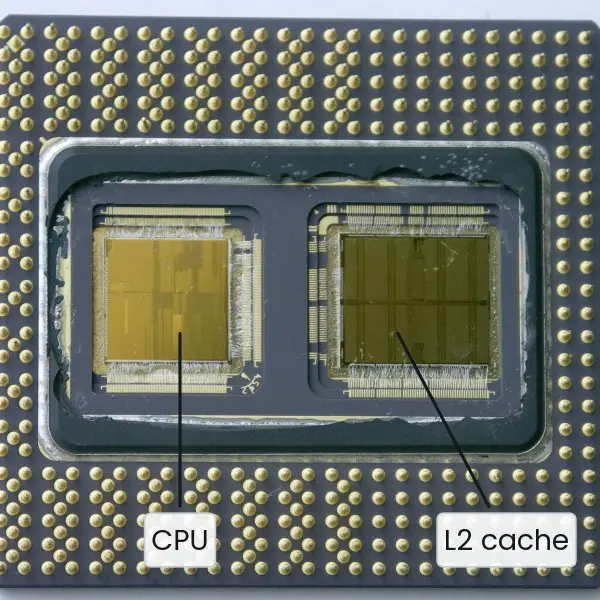
This section first shows the real devices (a plate of chips and a plate of a processor die and a hard disk), and then draws the ideas to scale: the hierarchy, a 1 KB address map, the three parts of one disk access, three cache mappings run on the same eight references, a split address, a page-table lookup, three replacement policies, Belady's anomaly and segmented paging.
All numbers in the figures were computed with a short Python program, not guessed.


7.7.1 Eight uses of caches, virtual memory and storage in Nepal
- Caches inside phone and laptop processors. Every Snapdragon or MediaTek phone sold in Kathmandu has L1 and L2 caches on the chip. They keep recently used instructions and data a few nanoseconds away from the core. This is why a loop in an app runs much faster than the slow DRAM alone would allow. Locality of reference is the reason the small cache works so well.
- Browser and proxy caches. A browser keeps recent pages, images and scripts on the disk or in memory so that a repeat visit loads in a moment. College networks and ISPs such as WorldLink and Vianet also use caching servers. A popular Nepali news site then does not need to cross the international link for every reader. This is the cache idea applied to the web.
- DRAM in banking and payment servers. Systems behind ConnectIPS and Fonepay hold the hot part of their data in DRAM so that a balance check is answered in microseconds. DRAM needs refresh and loses its data at power-off, so every change is also written to disk or SSD. The two levels together give both speed and safety. Banks also keep DRAM on error-correcting (ECC) modules.
- SSDs in office and college computers. Replacing a hard disk with an SSD removes the seek and rotational delay of Fig. 7.3. A TU computer lab or a cyber cafe that moves to SSDs sees Windows boot in seconds instead of minutes. The cost per bit is higher, so many machines use a small SSD for the system and a large disk for files.
- Virtual memory on lab PCs. A computer with 4 GB of RAM can still run a browser, an IDE and a document at once, because the operating system moves idle pages to the disk. When RAM is too small, the page-fault rate of Fig. 7.8 grows and the machine slows to a crawl. Students see this as thrashing when they open too many tabs.
- Flash and EEPROM in smart cards. The chip in a Nepali smart driving licence, e-passport or bank card stores a small amount of data in EEPROM or flash. The data survive without power and can be rewritten a limited number of times. This is the same technology as the erasable chips of Plate 7.1, made electrically erasable.
- ROM firmware in machines. An ATM, a voting machine, a router or a smart meter of the Nepal Electricity Authority starts from a program stored in ROM or flash. This boot program must be there at power-on, before any disk is read. The BIOS or UEFI of every PC is the same idea, and it is why a PC can start at all.
- Memory protection on shared servers. A server such as the TU examination or EMIS system runs many programs at once. Base and limit registers, page protection bits and kernel mode stop one program from reading or changing another program's memory. A bug in one user's program then causes a segmentation fault for that program only, and the system stays up.
Formula and fact sheet
- n address lines → 2ⁿ locations; chips needed = total size ÷ chip size.
- Disk capacity = surfaces × tracks × sectors × bytes; access = seek + rotational (½ revolution) + transfer; at 7200 rpm average latency 4.17 ms.
- AMAT = t_c + (1 − h) × t_m (= h·t_c + (1 − h)(t_c + t_m)).
- Direct-mapped split: offset = log₂(block size); index = log₂(lines); tag = address bits − index − offset. k-way: sets = lines ÷ k.
- Pages: offset = log₂(page size); page-table entries = 2^{page-number bits}.
- FIFO may show Belady's anomaly; LRU and OPT do not.
Chapter summary
- The hierarchy trades size, speed and cost; locality makes it work.
- SRAM for cache, DRAM for main memory, ROM family for non-volatile code; the address map and chip-select decode place chips in the address space.
- A disk's access time is dominated by seek and rotation.
- Caches map blocks by direct, fully associative or set-associative rules, replace by LRU/FIFO/random and write by write-through or write-back.
- Virtual memory pages programs on demand; page faults are handled by the OS using FIFO/LRU-like replacement; TLBs speed translation.
- Segmentation and segmented paging structure memory; base/limit registers and protection bits enforce isolation.
Practice
- Explain the memory hierarchy and the principle of locality.
- Differentiate between SRAM and DRAM; between PROM, EPROM and EEPROM.
- Design a memory address map for 1 KB RAM (four 256 × 8 chips) and 512 B ROM in an 11-bit address space.
- A disk has 4 surfaces, 500 cylinders, 40 sectors per track and 1 KB sectors, rotating at 6000 rpm. Find its capacity and the average rotational latency.
- A cache of 8 KB, 32-byte blocks, 24-bit addresses, direct-mapped: find offset, index, tag bits.
- A system has cache time 5 ns, memory time 60 ns, hit ratio 0.92. Find the average access time and the speed-up.
- Compare direct, associative and set-associative mapping.
- Distinguish write-through and write-back.
- For the string 1 2 3 2 4 1 5 2 1 2 3 4 with 3 frames, count page faults under FIFO and LRU.
- Explain paging, page tables, page faults and the role of the TLB. What is memory protection?
Answers and worked solutions
1. See 7.1: levels from registers to disk; locality (temporal and spatial) means the upper levels satisfy most accesses.
2. SRAM: flip-flop cells, fast, no refresh, used for cache; DRAM: capacitor cells, refresh needed, cheaper and denser, used for main memory. PROM: programmed once; EPROM: UV-erasable; EEPROM: electrically erasable per byte.
3. 1 KB RAM = 4 × 256 B ⇒ 8 address lines per chip; 512 B ROM needs 9 lines. In an 11-bit space (2 KB): A10 = 0 selects RAM, A10 = 1 ROM; A9–A8 → 2-to-4 decoder for the RAM chips; ranges RAM 000–0FF, 100–1FF, 200–2FF, 300–3FF; ROM 400–5FF.
4. Capacity = 4 × 500 × 40 × 1024 = 81,920,000 B. 6000 rpm → 10 ms per revolution → latency 5 ms.
5. Offset = 5 bits (32 B); lines = 8192/32 = 256 ⇒ index 8 bits; tag = 24 − 8 − 5 = 11 bits.
6. AMAT = 5 + 0.08 × 60 = 9.8 ns; speed-up = 60/9.8 ≈ 6.1.
7. Direct: one possible line, simple, conflict misses; associative: any line, no conflicts, costly comparators; set-associative: k lines per set, balanced.
8. Write-through updates cache and memory together; write-back updates only the cache and writes the dirty line back on eviction.
9. FIFO (frames after each fault): 1 F [1]; 2 F [1,2]; 3 F [1,2,3]; 2 H; 4 F [2,3,4]; 1 F [3,4,1]; 5 F [4,1,5]; 2 F [1,5,2]; 1 H; 2 H; 3 F [5,2,3]; 4 F [2,3,4] → 9 faults. LRU: 1 F; 2 F; 3 F; 2 H; 4 F (evict 1) [3,2,4]; 1 F (evict 3) [2,4,1]; 5 F (evict 2) [4,1,5]; 2 F (evict 4) [1,5,2]; 1 H; 2 H; 3 F (evict 5) [1,2,3]; 4 F (evict 1) [2,3,4] → also 9 faults. Both counts were checked by script; the two policies happen to tie on this string.
10. Pages/frames, per-process page table with valid bit; a page fault traps to the OS which loads the page; the TLB caches recent translations; memory protection uses base/limit registers and permission bits to confine each process.
Model answers for Unit 7
Q1. Explain the memory hierarchy and the principle of locality. Why is a hierarchy needed? (5 marks)
A processor can execute an instruction in about a nanosecond, but a DRAM access takes about 100 ns and a disk access about 10 ms.
No single technology is at the same time fast, large and cheap, so a computer uses a hierarchy of memories (Fig. 7.1).
Each level is smaller, faster and costlier per bit than the one below it, and it holds copies of the data most likely to be needed next.
| Level | Technology | Typical size | Access time |
|---|---|---|---|
| Registers | flip-flops in the CPU | hundreds of bytes | under 1 ns |
| L1, L2, L3 cache | SRAM on or near the CPU | 32 KB to 32 MB | 1 to 20 ns |
| Main memory | DRAM | 4 to 64 GB | 50 to 100 ns |
| Secondary | SSD or magnetic disk | 100 GB to TBs | 0.1 ms or 10 ms |
| Archive | tape, optical disc | very large | seconds |
The hierarchy works because of the principle of locality. Temporal locality says that an item used now is likely to be used again soon, as in a loop counter.
Spatial locality says that items near a used item are likely to be used soon, as in sequential instructions or the elements of an array.
Because of both, a whole block is copied up the hierarchy on a miss, and later references hit in the fast level.
For example, with a hit ratio of 0.9, a 10 ns cache in front of a 100 ns memory gives an average access time of 20 ns, five times faster than memory alone.
The user sees a memory almost as fast as the top level and almost as large and cheap as the bottom level.
Q2. Differentiate between SRAM and DRAM. Name the members of the ROM family. (5 marks)
Random-access memory is volatile: it loses its contents when the power goes off. It comes in two forms that differ in the cell used to store one bit.
| Point | SRAM (static RAM) | DRAM (dynamic RAM) |
|---|---|---|
| Cell | flip-flop of about 6 transistors | one transistor and one capacitor |
| Refresh | not needed | needed every few milliseconds |
| Speed | fast (1 to 10 ns) | slower (50 to 100 ns) |
| Density and cost | low density, costly per bit | high density, cheap per bit |
| Power | low when idle | refresh uses power |
| Use | cache and registers | main memory (SDRAM, DDR4, DDR5) |
DRAM stores a bit as charge on a tiny capacitor. The charge leaks away, so a refresh circuit reads and rewrites every row regularly; reading is also destructive and must be followed by a write-back.
SRAM keeps its value as long as power is on, but its cell is large, so a chip holds far fewer bits (Plate 7.1).
ROM is non-volatile and holds the boot program. ROM proper is programmed at the factory. PROM is programmed once by the user. EPROM is erased by ultraviolet light through its quartz window and can be reprogrammed.
EEPROM is erased electrically, one byte at a time, and is used for settings. Flash is a block-erasable EEPROM used in SSDs, pen drives and phones. In every case the data stay without power.
Q3. Explain cache memory. Describe the three mapping functions, the replacement policies and the write policies. (10 marks)
A cache is a small, fast SRAM placed between the CPU and main memory. It holds copies of the blocks (lines) most recently used. When the CPU needs a word, the cache is searched first.
If the word is there it is a hit; if not, it is a miss and the whole block is fetched from memory and placed in the cache. If the hit ratio is h, the average access time is t_cache + (1 − h) × t_memory.
For a 10 ns cache, 100 ns memory and h = 0.9 this is 10 + 0.1 × 100 = 20 ns, a speed-up of 5 over memory alone.
Mapping. Every cache line stores a tag that says which memory block it holds, and a valid bit.
- Direct mapping: block j goes to line (j mod number of lines). It is simple and fast, but two active blocks that share a line evict each other (a conflict miss).
- Fully associative: a block may go to any line, so there are no conflicts, but the tag must be compared with all lines at once, which needs many comparators.
- Set-associative (k-way): block j goes to set (j mod number of sets) and may use any of the k lines of that set. It is the usual compromise (2-, 4- and 8-way).
For a 1 KB cache with 16-byte lines and 16-bit addresses, the direct-mapped address is tag 6 bits, index 6 bits, offset 4 bits (Fig. 7.5).
Running the references 0, 8, 0, 6, 8, 0, 8, 6 in a four-line cache (Fig. 7.4) gives 1 hit for direct mapping, 2 for two-way and 5 for fully associative.
Replacement. When a set is full a victim must be chosen: LRU (least recently used, best in practice), FIFO, random, or LFU. A direct-mapped cache needs no policy.
Write policies.
| Policy | Action | Remarks |
|---|---|---|
| Write-through | write cache and memory together | memory always correct, but slow without a write buffer |
| Write-back | write cache only and set the dirty bit; write memory when the line is evicted | far fewer memory writes, but harder with several cores |
| Write-allocate | load the block on a write miss | usually paired with write-back |
In conclusion, the cache is the main reason a modern processor runs near its own speed instead of the speed of DRAM.
Q4. Explain virtual memory. How are paging, the page table, a page fault and the TLB related? (10 marks)
Virtual memory gives each program the illusion of a large, private, contiguous memory, larger than the installed RAM, by keeping the program on disk and loading only the needed pages into RAM. It lets many programs run at once and keeps them separate.
Paging. The virtual address space is cut into equal pages (commonly 4 KB) and physical memory into frames of the same size. The CPU produces a virtual address = page number + offset.
The memory-management unit (MMU) replaces the page number by a frame number and keeps the offset (Fig. 7.6).
Page table. Each process has a page table with one entry per page. An entry holds the frame number, a valid (present) bit, and protection and dirty bits.
For a 32-bit address and 4 KB pages, the offset is 12 bits and the page number is 20 bits, so the table has 2^{20} = 1,048,576 entries, or 4 MB with 4-byte entries (so real systems use multi-level tables).
For virtual address 00003A7CH, page 3 maps to frame 1BH, so the physical address is 0001BA7CH.
Page fault and demand paging. If the valid bit is 0, the access causes a page fault, a trap to the operating system. The OS:
- checks that the address is legal,
- finds a free frame, or evicts a victim page (writing it back if dirty),
- reads the wanted page from disk,
- updates the page table, and
- restarts the faulting instruction.
A fault costs milliseconds, so the effective access time is (1 − p) × t_mem + p × t_fault. With t_mem = 100 ns and t_fault = 8 ms, a fault rate of 1 in 1000 gives 8,100 ns, which is 81 times slower (Fig. 7.8).
TLB. Every access would need two memory reads (page table, then data). A translation lookaside buffer is a small associative cache of recent page-table entries.
With a 98% TLB hit ratio, 10 ns TLB time and 100 ns memory, the average translation-plus-access time is 0.98 × (10 + 100) + 0.02 × (10 + 200) = 112 ns instead of 200 ns.
Replacement and thrashing. FIFO, LRU and optimal policies choose the victim; if too many processes compete for memory the system thrashes, spending its time on faults, and the OS reduces the number of active processes.
Q5. For the reference string 2 3 2 1 5 2 4 5 3 2 5 2 with three frames, find the number of page faults under FIFO, LRU and Optimal. (5 marks)
Each page is brought in on first use. F means a fault and h a hit. The frames are shown after each reference.
FIFO (evict the oldest page): 2 F [2]; 3 F [2,3]; 2 h; 1 F [2,3,1]; 5 F (evict 2) [3,1,5]; 2 F (evict 3) [1,5,2]; 4 F (evict 1) [5,2,4]; 5 h; 3 F (evict 5) [2,4,3]; 2 h; 5 F (evict 2) [4,3,5]; 2 F (evict 4) [3,5,2]. Total 9 faults.
LRU (evict the page unused longest): 2 F; 3 F; 2 h; 1 F [3,2,1]; 5 F (evict 3) [2,1,5]; 2 h; 4 F (evict 1) [5,2,4]; 5 h; 3 F (evict 2) [4,5,3]; 2 F (evict 4) [5,3,2]; 5 h; 2 h. Total 7 faults.
Optimal (evict the page whose next use is furthest away): 2 F; 3 F; 2 h; 1 F [2,3,1]; 5 F (evict 1, which is never used again) [2,3,5]; 2 h; 4 F (evict 2, next used at the tenth reference, after 5 and 3) [4,3,5]; 5 h; 3 h; 2 F (evict 4, never used again) [2,3,5]; 5 h; 2 h. Total 6 faults.
| Policy | Faults | Hit ratio (12 references) |
|---|---|---|
| FIFO | 9 | 3/12 = 25% |
| LRU | 7 | 5/12 = 41.7% |
| Optimal | 6 | 6/12 = 50% |
Optimal is the lower bound because it needs future knowledge, so it is only a yardstick (Fig. 7.7 shows another string). LRU is close to it in practice.
FIFO is the simplest but can show Belady's anomaly: for the string 1 2 3 4 1 2 5 1 2 3 4 5, FIFO gives 9 faults with three frames and 10 with four (Fig. 7.8).
Q6. A disk has 4 surfaces, 500 cylinders, 40 sectors per track and 1 KB sectors, and rotates at 6000 rpm. The average seek time is 8 ms. Find its capacity, average rotational latency, and the average time to read one sector. (5 marks)
A hard disk stores data on concentric tracks. All the tracks at the same arm position, one per surface, form a cylinder, and each track is cut into sectors (Fig. 7.3).
Capacity = surfaces × cylinders × sectors per track × bytes per sector = 4 × 500 × 40 × 1024 = 81,920,000 bytes, about 81.9 MB (78.1 MiB). There are 4 × 500 = 2000 tracks and 80,000 sectors.
Rotational latency. At 6000 rpm one revolution takes 60 / 6000 s = 10 ms. On average the wanted sector is half a turn away, so the average latency is 5 ms.
Transfer time. In one revolution (10 ms) the head passes all 40 sectors, so one sector passes in 10 / 40 = 0.25 ms. The transfer rate is 40 KB per 10 ms = 4.096 MB/s.
Access time = seek + rotational latency + transfer = 8 + 5 + 0.25 = 13.25 ms.
| Part | Time | Share |
|---|---|---|
| Seek | 8 ms | 60.4% |
| Rotation | 5 ms | 37.7% |
| Transfer | 0.25 ms | 1.9% |
Seek and rotation together make 98% of the time, which is why the operating system schedules requests to cut the arm movement, reads whole blocks, and keeps frequently used data in a cache. An SSD has no moving parts, so it removes both of these delays.
Q7. Design a memory address map for 1 KB of RAM using four 256 x 8 chips and 512 bytes of ROM in an 11-bit address space. (5 marks)
An 11-bit address gives 2^{11} = 2048 locations (000H to 7FFH). A 256 x 8 RAM chip needs 8 address lines (2^{8} = 256) and the 512 x 8 ROM needs 9 lines (2^{9} = 512).
The lines are used as follows (Fig. 7.2 shows the same idea for 10 bits).
- A7 to A0 (8 lines) go to every RAM chip to choose a byte inside the chip.
- A9 and A8 go to a 2-to-4 decoder whose four outputs are the chip-select (CS) inputs of RAM 1 to RAM 4.
- A10 chooses the device type: A10 = 0 enables the RAM decoder and A10 = 1 enables the ROM.
- The ROM uses A8 to A0 inside the chip. Because it only needs nine lines, A10 = 1 together with A9 = 0 gives the block 400H to 5FFH, and the next block 600H to 7FFH is a mirror of it (or is left unused).
| Component | A10 | A9 A8 | A7 to A0 | Address range |
|---|---|---|---|---|
| RAM 1 | 0 | 00 | x | 000H to 0FFH |
| RAM 2 | 0 | 01 | x | 100H to 1FFH |
| RAM 3 | 0 | 10 | x | 200H to 2FFH |
| RAM 4 | 0 | 11 | x | 300H to 3FFH |
| ROM | 1 | 0x | x | 400H to 5FFH |
Check: four chips of 256 bytes give 1024 = 400H bytes, so the RAM ends at 3FFH and the ROM starts at 400H. If the CPU must find its boot program at address 0, as many processors do, the two blocks are simply swapped by inverting A10 in the select logic.