Chapter 21 · Modern Physics · 2 questions in the paper · 29 min read
Semiconductors and Logic Gates
What the syllabus asks for 3
- Energy bands in metals, semiconductors and insulators; intrinsic and extrinsic semiconductors
- The p–n junction diode, its biasing and its use as a rectifier
- Logic gates: AND, OR, NOT, NAND and NOR
This is the chapter behind every phone charger, solar panel and calculator in Nepal. Modern Physics carries 12 of the 50 Physics questions (official MEC weightage), and we estimate about 2 come from here. The paper asks three kinds of question: one fact about bands or doping (which carrier is in the majority, what a donor does), one about the diode (which way it conducts, what the reverse current is, what a rectifier puts out), and one about a gate (read a truth table, identify a gate from its output, or know which gates are universal). Almost nothing here needs a long calculation — but the definitions must be exact, because the distractors are built from half-remembered versions of them.
- Band picture: a full valence band, an empty conduction band, and the gap between them; E_g\\approx0 for a metal, about 1 eV for a semiconductor, more than 3 eV for an insulator.
- Intrinsic: n_e=n_h=n_i, conduction by electron–hole pairs, resistance falls as temperature rises.
- Extrinsic: pentavalent donor gives n-type (electrons majority), trivalent acceptor gives p-type (holes majority); the donor level sits just below the conduction band, the acceptor level just above the valence band.
- Mass action law n_en_h=n_i^2; charge neutrality; conductivity \sigma=e(n_e\mu_e+n_h\mu_h).
- The p–n junction: diffusion, recombination, the depletion layer of immobile ions, the barrier potential (Si 0.7 V, Ge 0.3 V).
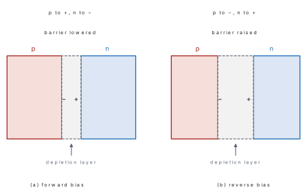
- Forward bias narrows the depletion layer and lowers the barrier; reverse bias widens it and raises it. Reverse current is minority-carrier drift, small but not zero.
- Rectifiers: one diode for half-wave, two (centre tap) or four (bridge) for full-wave; output frequency f or 2f; average V_0/\pi or 2V_0/\pi.
- Gates AND, OR, NOT, NAND, NOR with truth tables; NAND and NOR are universal; XOR is not.
21.1 Energy bands in metals, semiconductors and insulators; intrinsic and extrinsic semiconductors
21.1.1 From atomic levels to bands
An isolated atom has sharp energy levels. In a solid, a vast number of atoms are packed within a few nanometres, and the Pauli exclusion principle forbids two electrons from sharing the same state. Each atomic level therefore splits into a band of closely spaced levels — so closely spaced that the electron sees an almost continuous range of allowed energies.
Two bands matter:
- the valence band, formed from the outer electrons that are bound to atoms;
- the conduction band, the next band up, in which electrons are free to move through the crystal and carry current.
Between them lies the forbidden energy gap E_g, where no electron state exists. The size of that gap decides what the material is.
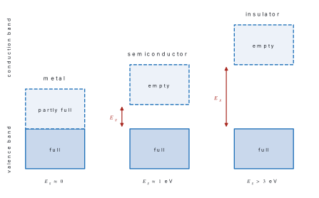
| Solid | E_g | Conduction at room temperature | Resistance when heated |
|---|---|---|---|
| Metal (Cu, Ag, Al) | zero — bands overlap or the top band is partly full | abundant free electrons | increases (lattice vibrations scatter them) |
| Semiconductor (Ge, Si) | 0.7 eV (Ge), 1.1 eV (Si) | small but useful; a few electrons per 10^{9} atoms are free | decreases (many more carriers are freed) |
| Insulator (diamond, glass) | about 5.5 eV (diamond), more than 3 eV generally | effectively none | stays negligible until breakdown |
The different sign of the temperature coefficient is the fastest way to tell a semiconductor from a metal in an exam question: a metal gets worse when hot, a semiconductor gets better.
21.1.2 Intrinsic semiconductors
A pure semiconductor is called intrinsic. At absolute zero every electron sits in the valence band, the conduction band is empty, and the crystal is an insulator. At room temperature thermal energy frees a small number of electrons, each leaving behind a vacancy in a covalent bond. That vacancy behaves as a positive carrier called a hole: an electron from a neighbouring bond can move into it, so the hole appears to move the other way.
In a pure crystal every freed electron leaves one hole, so
where n_i is the intrinsic carrier concentration. For silicon at 300 K it is about 1.5\times10^{16} m⁻³ — tiny compared with the 5\times10^{28} atoms per cubic metre, which is why pure silicon is a poor conductor.
Two consequences worth memorising:
- conduction in an intrinsic semiconductor is by electrons and holes together, and the two currents add;
- as the temperature rises, n_i rises very rapidly (roughly doubling every 10 K near room temperature), so the resistance falls.
21.1.3 Extrinsic semiconductors: doping
A controlled tiny addition of an impurity — about one atom in 10^{6} — raises the carrier concentration enormously. This is doping, and the result is an extrinsic semiconductor.
n-type. Add a pentavalent atom (phosphorus, arsenic, antimony) to silicon. Four of its five outer electrons form covalent bonds; the fifth is loosely bound and needs only about 0.01–0.05 eV to enter the conduction band. The impurity donates an electron, so it is a donor, and the crystal becomes n-type: electrons are the majority carriers and holes the minority carriers. The donor level lies just below the conduction band. The crystal stays electrically neutral — every donor also leaves a fixed positive ion behind.
p-type. Add a trivalent atom (boron, aluminium, gallium, indium). It has one bond too few, so it accepts an electron from a neighbouring bond, creating a hole. The impurity is an acceptor, and the crystal becomes p-type: holes are the majority carriers, electrons the minority. The acceptor level lies just above the valence band.
| n-type | p-type | |
|---|---|---|
| Dopant | pentavalent (P, As, Sb) | trivalent (B, Al, Ga, In) |
| Impurity called | donor | acceptor |
| Majority carrier | electrons | holes |
| Minority carrier | holes | electrons |
| Impurity level | just below the conduction band | just above the valence band |
| Net charge of the crystal | zero | zero |
A doped crystal is neutral. Each donor atom gives a free electron and leaves a positive ion; each acceptor takes an electron and leaves a negative ion. The two charges cancel. Students often write "n-type is negatively charged" — that is wrong, and it is a standard distractor.
21.1.4 Mass action law and conductivity
In thermal equilibrium the product of the two carrier concentrations is fixed by the temperature and the material:
This is the mass action law. It says that if doping increases one kind of carrier, the other must fall by the same factor. Dope silicon (n_i=1.5\times10^{16} m⁻³) so that n_e=4.5\times10^{22} m⁻³, and the hole concentration drops to
The conductivity of a semiconductor is the sum of the two contributions:
where \mu_e and \mu_h are the mobilities (m² V⁻¹ s⁻¹). In an n-type material the first term dominates; in a p-type material the second does. Because electrons move more easily than holes, \mu_e>\mu_h in both silicon and germanium.
Problem. A silicon sample is doped so that n_e=5.0\times10^{22} m⁻³. Taking \mu_e=0.05 m² V⁻¹ s⁻¹, find its conductivity and resistivity. (The hole contribution is negligible here.)
Solution. \sigma=en_e\mu_e=(1.6\times10^{-19})(5.0\times10^{22})(0.05) =400 S m⁻¹.
\rho=1/\sigma=1/400=2.5\times10^{-3} Ω m.
Check. Intrinsic silicon has \sigma of order 10^{-3} S m⁻¹, so doping has raised the conductivity by about six powers of ten. That is why a doped crystal is useful and a pure one is not.
21.2 The p–n junction diode, its biasing and its use as a rectifier
21.2.1 How the junction forms
Join a p-type and an n-type crystal. At the boundary, holes diffuse from p to n and electrons diffuse from n to p, because each side has far more of its own carrier than the other. The carriers that cross recombine, so a thin layer on each side is left with no free carriers but with the fixed ions the dopants left behind: negative acceptor ions on the p side, positive donor ions on the n side.
This is the depletion region (or depletion layer). It contains a built-in electric field pointing from the positive ions to the negative ions — that is, from n to p — and a corresponding potential barrier that opposes further diffusion. Equilibrium is reached when the drift of the few remaining carriers exactly balances the diffusion. The barrier height is about 0.7 V for silicon and 0.3 V for germanium.
21.2.2 Forward and reverse bias
Forward bias. Connect the p side to the positive terminal and the n side to the negative terminal. The applied field opposes the built-in field, so the barrier is lowered, the depletion region narrows, and majority carriers are pushed towards the junction in large numbers. Once the applied voltage exceeds the barrier, the current rises very steeply. The diode behaves like a closed switch with a small resistance.
Reverse bias. Connect the p side to the negative terminal and the n side to the positive terminal. The applied field adds to the built-in field, the barrier is raised, and the depletion region widens. Majority carriers are pulled away from the junction and cannot cross. Only the minority carriers — the few holes on the n side and electrons on the p side — are swept across by the field, giving a tiny reverse saturation current. It is of order microamperes in germanium and nanoamperes in silicon, and it hardly changes with the applied voltage because it depends on how many minority carriers exist, not on how hard they are pushed.
21.2.3 The I–V characteristic
| Region | Behaviour | Why |
|---|---|---|
| Forward, V below about 0.5 V (Si) | almost no current | the applied voltage has not yet cancelled the barrier |
| Forward, V above the knee (0.7 V for Si, 0.3 V for Ge) | current rises exponentially | the barrier is gone and the junction conducts freely |
| Reverse, small V | tiny current, nearly constant | minority carriers only |
| Reverse, beyond the breakdown voltage | current increases sharply | avalanche or Zener breakdown |
Two things follow that questions test constantly:
- a diode is not a resistor: its resistance is very large in reverse and very small in forward, and it changes with the applied voltage;
- the reverse saturation current is not zero. It is the drift of minority carriers, and it is the reason a reverse-biased diode still leaks a little.
Breakdown. At a large reverse voltage the field in the depletion region becomes strong enough to do one of two things. In avalanche breakdown (lightly doped junctions, higher voltages) the few accelerated carriers knock more electrons out of atoms, and the number multiplies. In Zener breakdown (heavily doped junctions, below about 6 V) the field is strong enough to pull electrons straight out of their bonds by tunnelling. Both are reversible if the current is limited, which is why a Zener diode is used as a voltage reference.
21.2.4 The diode as a rectifier
A rectifier converts alternating current into direct current by letting one half of each cycle through and blocking the other. The diode is ideal for the job because it conducts in one direction only.
Half-wave rectifier. One diode in series with the load. Current flows only during the half cycle in which the diode is forward biased; the other half is blocked, so the output is a series of pulses with gaps.
Full-wave rectifier. Either two diodes with a centre-tapped transformer, or four diodes in a bridge. Both halves of the input reach the load in the same direction, so the gaps are filled and the output pulses come twice as often.
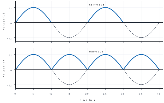
| Half-wave | Full-wave (centre tap) | Full-wave (bridge) | |
|---|---|---|---|
| Diodes | 1 | 2 | 4 |
| Conducts on | one half cycle | both half cycles | both half cycles |
| Output frequency | f | 2f | 2f |
| Average output | V_0/\pi\approx0.318V_0 | 2V_0/\pi\approx0.637V_0 | 2V_0/\pi\approx0.637V_0 |
| Ripple factor | 1.21 | 0.48 | 0.48 |
| Efficiency (maximum) | 40.6 % | 81.2 % | 81.2 % |
Here V_0 is the peak value of the input. The average is not V_0/\sqrt{2}: that is the rms value of a full sine wave, and it belongs to a different question.
The output is pulsating DC, not the steady voltage of a battery. A reservoir capacitor across the load charges to the peak and fills the gaps, which is why a real charger gives a nearly steady output. Also: a rectifier does not change the frequency of the supply into anything other than the pulse rate — the output pulses are at f (half-wave) or 2f (full-wave).
Problem. A silicon diode (barrier 0.7 V) is in series with a 100 Ω resistor and a 5.0 V battery. Find the current.
Solution. The diode drops about 0.7 V, so the voltage across the resistor is 5.0-0.7=4.3 V.
I=\dfrac{4.3}{100}=0.043 A =43 mA.
Check. If the diode were reversed, the current would be only the reverse saturation current — microamperes — and the answer would be about a million times smaller.
21.3 Logic gates: AND, OR, NOT, NAND and NOR
21.3.1 Boolean variables and truth tables
A logic gate is a circuit with one output and one or more inputs, where every signal is either 0 (low, about 0 V) or 1 (high, about 5 V). A truth table lists the output for every possible combination of inputs. With n inputs there are 2^n rows.
21.3.2 The five gates
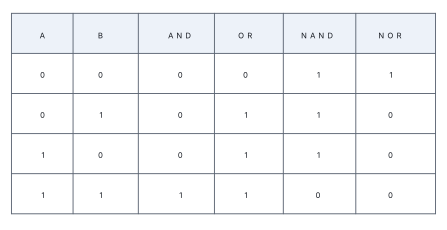
AND. The output is 1 only when all inputs are 1. Written Y=A\cdot B. Think of two switches in series: the lamp lights only if both are closed.
OR. The output is 1 when at least one input is 1. Written Y=A+B. Two switches in parallel.
NOT. One input, and the output is its opposite: Y=\bar A. It is also called an inverter.
NAND. AND followed by NOT: Y=\overline{A\cdot B}. Its output is 0 only when all inputs are 1.
NOR. OR followed by NOT: Y=\overline{A+B}. Its output is 1 only when all inputs are 0.
21.3.3 Universal gates
A gate is universal if any other gate can be built from copies of it alone. NAND and NOR are universal; AND, OR and XOR are not.
- NOT from NAND: join both inputs together. Then Y=\overline{A\cdot A}=\bar A.
- AND from NAND: a NAND followed by a NAND used as a NOT.
- OR from NAND: invert both inputs first, then NAND them: \overline{\bar A\cdot\bar B}=A+B by De Morgan.
De Morgan's theorems make these manipulations possible:
NAND is "not all ones": output 0 only for 11. NOR is "not any one": output 1 only for 00.
21.3.4 A worked combination: XOR from four NAND gates
The XOR (exclusive-OR) gate gives 1 when the inputs are different and 0 when they are the same. Its expression is
It is the gate that adds without carrying, and it is the heart of a half adder.
Build it from four NAND gates. Label the gates N1 to N4.
- N_1=\overline{AB} — the NAND of the inputs.
- N_2=\overline{A\cdot N_1}=\overline{A\cdot\overline{AB}}
- N_3=\overline{B\cdot N_1}=\overline{B\cdot\overline{AB}}
- Y=N_4=\overline{N_2\cdot N_3}
Check the four cases:
| A | B | N_1 | N_2 | N_3 | Y |
|---|---|---|---|---|---|
| 0 | 0 | 1 | 1 | 1 | 0 |
| 0 | 1 | 1 | 1 | 0 | 1 |
| 1 | 0 | 1 | 0 | 1 | 1 |
| 1 | 1 | 0 | 1 | 1 | 0 |
The output column is 0, 1, 1, 0: exactly XOR. Algebraically, \overline{N_2N_3}=\overline{\bar A\bar B\cdot\bar AB}=A\bar B+\bar AB, which is the XOR expression.
NAND is universal, XOR is not. Four NAND gates make an XOR; no number of XOR gates can make an AND or an OR, because XOR always gives 0 for equal inputs. And a two-input XOR with both inputs joined gives a constant 0 — it cannot even invert.
Problem. A signal A is fed to both inputs of a NAND gate. The output then goes to one input of an AND gate, whose other input is B. Write the final output and evaluate it for A=1, B=1.
Solution. The NAND with joined inputs is a NOT, so its output is \bar A. The AND gate then gives Y=\bar A\cdot B.
For A=1, B=1: \bar A=0, so Y=0\cdot1=0.
Formula and fact sheet
| Item | Fact or formula |
|---|---|
| Band gap | metal \approx0; Ge 0.7 eV, Si 1.1 eV, GaAs 1.4 eV; insulator > 3 eV (diamond 5.5 eV) |
| Gap and wavelength | E_g=hc/\lambda, so \lambda_{max}=1240/E_g(\text{eV}) nm |
| Intrinsic | n_e=n_h=n_i; Si n_i\approx1.5\times10^{16} m⁻³ at 300 K; resistance falls with temperature |
| n-type | pentavalent donor (P, As, Sb); electrons majority; donor level just below E_c |
| p-type | trivalent acceptor (B, Al, Ga, In); holes majority; acceptor level just above E_v |
| Mass action | n_en_h=n_i^2 |
| Conductivity | \sigma=e(n_e\mu_e+n_h\mu_h), \rho=1/\sigma |
| Junction | diffusion → recombination → depletion layer of immobile ions → barrier |
| Barrier potential | Si 0.7 V, Ge 0.3 V |
| Forward bias | p to +, depletion narrows, barrier falls, current large |
| Reverse bias | p to −, depletion widens, barrier rises, current = minority-carrier drift (µA or nA) |
| Breakdown | avalanche (impact ionisation) or Zener (tunnelling, heavily doped, < 6 V) |
| Half-wave | 1 diode; output at f; average V_0/\pi=0.318V_0; ripple factor 1.21; efficiency 40.6 % |
| Full-wave | 2 diodes (centre tap) or 4 (bridge); output at 2f; average 2V_0/\pi=0.637V_0; ripple 0.48; efficiency 81.2 % |
| Gate expressions | AND A\cdot B; OR A+B; NOT \bar A; NAND \overline{AB}; NOR \overline{A+B}; XOR A\bar B+\bar AB |
| Gate outputs | AND: 1 only for 11. OR: 1 for 01, 10, 11. NAND: 0 only for 11. NOR: 1 only for 00 |
| Universal gates | NAND and NOR only |
| De Morgan | \overline{AB}=\bar A+\bar B; \overline{A+B}=\bar A\cdot\bar B |
| XOR from NAND | 4 NAND gates; half-adder: sum = XOR, carry = AND |
Chapter summary
- In a solid the atomic levels broaden into bands; the valence band is full, the conduction band is where moving electrons live, and the gap between them decides the class of the solid.
- Metals have no gap (or overlapping bands) and their resistance rises with temperature; semiconductors have E_g of about 1 eV and their resistance falls; insulators have E_g>3 eV.
- In an intrinsic semiconductor n_e=n_h=n_i, and conduction is by electron–hole pairs created by thermal energy.
- A pentavalent donor makes an n-type crystal (electrons majority); a trivalent acceptor makes a p-type crystal (holes majority). The crystal stays neutral, and n_en_h=n_i^2.
- At a p–n junction, diffusion and recombination leave a depletion layer of fixed ions and a barrier of 0.7 V (Si) or 0.3 V (Ge).
- Forward bias narrows the depletion layer and lowers the barrier; reverse bias widens it and raises it. The reverse current is a small minority-carrier drift, not zero, and a diode's resistance is not constant.
- A diode rectifies: one diode gives half-wave output at f with average 0.318V_0; two or four give full-wave output at 2f with average 0.637V_0.
- AND gives 1 only for 11; OR gives 1 for any 1; NOT inverts; NAND is the negation of AND; NOR the negation of OR.
- NAND and NOR are universal. XOR (A\bar B+\bar AB) is not, and it takes four NAND gates to build one.
Practice questions
Set A — Recall (24 questions)
- In a metal at room temperature the conduction band isacompletely emptybcompletely fullcpartly filleddseparated by a gap of 3 eV
- The forbidden energy gap of a typical insulator isaabout 0.1 eVbmore than 3 eVcabout 1.1 eVdzero
- The energy gaps of silicon and germanium are abouta0.7 eV and 1.1 eVb5.5 eV and 3.0 eVc1.1 eV and 5.5 eVd1.1 eV and 0.7 eV
- Doping silicon with phosphorus producesaan n-type semiconductorba p-type semiconductorcan intrinsic semiconductordan insulator
- In a p-type semiconductor the majority carriers areaelectronsbpositive ionscholesdprotons
- A pentavalent impurity atom in silicon is calledaan acceptorba donorca recombination centredan intrinsic carrier
- The mass action law for a semiconductor in equilibrium isan_en_h=n_ibn_e+n_h=n_i^2cn_e/n_h=n_i^2dn_en_h=n_i^2
- The barrier potential of a silicon p–n junction is abouta0.7 Vb0.3 Vc1.1 Vd5.0 V
- In forward bias the p-side of a diode is connected to theanegative terminalbpositive terminalcearthdcase
- When a p–n junction is reverse biased, the depletion regionadisappearsbnarrowscwidensdstays the same width
- The reverse saturation current of a diode is carried byaminority carriersbmajority carrierscthe fixed ionsdthe battery only
- A half-wave rectifier usesafour diodesbtwo diodescno diodedone diode
- A full-wave rectifier is fed with 60 Hz AC. Its output pulses are ata30 Hzb60 Hzc120 Hzd240 Hz
- The Boolean expression for an AND gate isaA+Bb\bar AcA\cdot Bd\overline{A\cdot B}
- The output of a NOR gate is 1 whenaboth inputs are 0bboth inputs are 1cat least one input is 1dthe inputs are different
- Which of the following is a universal gate?aANDbORcXORdNAND
- The number of NAND gates needed to build an XOR gate isatwobfourcthreedsix
- A NOT gate is also calledaan inverterba buffercan adderda rectifier
- A two-input gate gives output 1 only when both inputs are 1. The gate isaORbNORcANDdNAND
- De Morgan's theorem may be written asa\overline{A+B}=\bar A+\bar BbA\cdot B=A+BcA+0=1d\overline{A\cdot B}=\bar A+\bar B
- In an intrinsic semiconductor, the number of holes isaequal to the number of conduction electronsbgreater than the number of electronscless than the number of electronsdzero at all temperatures
- As the temperature of a semiconductor rises, its resistanceaincreasesbdecreasescstays the samedbecomes infinite
- A hole in a semiconductor isaa free protonba positive ionca vacant bond that behaves as a positive chargeda positron
- At absolute zero the conduction band of a pure semiconductor isahalf filledbcompletely fullcpartly filleddcompletely empty
Answers and explanations — Set A
1. (c) — in a metal the highest band is only partly occupied (or two bands overlap), so electrons can move into empty states just above the filled ones. That is why metals conduct well.
2. (b) — insulators such as diamond have gaps of several electron volts (diamond about 5.5 eV), far more than thermal energy at room temperature.
3. (d) — silicon 1.1 eV, germanium 0.7 eV. Germanium's smaller gap is why it conducts more at the same temperature.
4. (a) — phosphorus is pentavalent: it donates its fifth electron, so electrons become the majority carriers and the crystal is n-type.
5. (c) — the trivalent acceptor takes an electron and leaves a hole, so holes dominate in p-type material.
6. (b) — a pentavalent atom donates an electron to the conduction band, hence "donor".
7. (d) — in equilibrium the product of the concentrations is fixed: n_en_h=n_i^2.
8. (a) — 0.7 V for silicon, 0.3 V for germanium. The barrier is set by the material, not by the applied voltage.
9. (b) — forward bias means p to the positive terminal, which lowers the barrier and lets holes and electrons flow towards the junction.
10. (c) — the applied field adds to the built-in field and pulls majority carriers away, so the depletion layer widens.
11. (a) — only minority carriers are available to be swept across in reverse bias, so the current is tiny.
12. (d) — one diode blocks one half of each cycle; two (centre tap) or four (bridge) are needed for full-wave.
13. (c) — both halves are used, so there are two pulses per cycle: 2\times60=120 Hz.
14. (c) — AND is logical multiplication, Y=A\cdot B; A+B is OR and \overline{A\cdot B} is NAND.
15. (a) — NOR is the negation of OR, and OR is 0 only when both inputs are 0, so NOR is 1 only for 00.
16. (d) — NAND (like NOR) can build every other gate, so it is universal; AND, OR and XOR cannot.
17. (b) — four NAND gates: one to form \overline{AB} and three to combine it into A\bar B+\bar AB.
18. (a) — the NOT gate inverts its single input, hence "inverter".
19. (c) — that is the definition of AND. NAND gives 0 for 11, and OR gives 1 for 01 and 10 as well.
20. (d) — the NAND of A and B equals \bar A+\bar B; the dual form is \overline{A+B}=\bar A\cdot\bar B, not \bar A+\bar B.
21. (a) — every thermally freed electron leaves one hole, so the two concentrations are equal in a pure crystal.
22. (b) — heating frees many more electron–hole pairs, and the rise in carriers outweighs the extra scattering, so resistance falls.
23. (c) — a hole is not a particle but a missing electron in a covalent bond; it behaves as a positive carrier because neighbouring electrons move into it.
24. (d) — at 0 K no electron has enough thermal energy to cross the gap, so the conduction band is empty and the crystal behaves as an insulator.
Set B — Understanding (14 questions)
- The energy gap of a semiconductor is much smaller than that of an insulator. The practical result at room temperature is thatano electrons can ever cross the gapba small fraction of electrons is thermally excited across itcthe valence band becomes emptydthe material becomes a metal
- Adding a trivalent impurity to silicon makes it p-type because the impurity atomadonates an extra electronbhas one electron too manycrepels electronsdaccepts an electron and leaves a hole
- In an n-type semiconductor the donor level liesajust below the conduction bandbjust above the valence bandcat the centre of the gapdinside the conduction band
- When a p–n junction is formed, the electrons and holes near the boundaryaare pushed apart by the batterybstay where they arecdiffuse across and recombine, leaving fixed ionsdform a metal layer
- A reverse-biased diode carries only a very small current becauseathe barrier disappearsbonly minority carriers are available to crosscthe junction becomes an insulatordthe battery is disconnected
- The resistance of a forward-biased diode isavery large and constantbinfinitecequal to that of the wiredsmall and not constant
- In the output of a half-wave rectifier, the current is zero duringano part of the cycleba quarter of each cyclecone half of each cycledthe whole cycle
- If one diode of a bridge rectifier is connected the wrong way round, the output isazero, and the supply may be shortedbhalf-wave rectifiedcunchangedddoubled
- An XOR gate gives output 1 whenaboth inputs are 1bthe two inputs are differentcboth inputs are 0dat least one input is 1
- A NAND gate with both inputs joined together acts asaan OR gateban AND gateca bufferda NOT gate
- The output of a two-input NAND gate with inputs 1 and 0 isa1b0cundefineddequal to the input 1
- Compared with a half-wave rectifier, a full-wave rectifier produces output pulses atahalf the frequencybthe same frequencyctwice the frequencydfour times the frequency
- A germanium diode conducts at a lower forward voltage than a silicon diode because germanium hasaa larger band gapba smaller band gapcmore free electrons than silicon at 0 Kdno depletion region
- The output of an AND gate is 1 only whenaany one input is 1bno input is 1cexactly one input is 1dall its inputs are 1
Answers and explanations — Set B
1. (b) — the gap is only about 1 eV, and thermal energy at 300 K is enough to lift a small fraction of electrons across it. An insulator's gap of several eV is not bridged at all.
2. (d) — the trivalent atom has only three valence electrons for four bonds, so it takes an electron from a neighbour and leaves a hole; that is an acceptor.
3. (a) — a donor's extra electron is only loosely bound, so its level sits just below the conduction band and is easily ionised.
4. (c) — majority carriers diffuse down their concentration gradient, recombine, and leave behind the immobile dopant ions that form the depletion layer.
5. (b) — the barrier is raised, so majority carriers cannot cross; only the few minority carriers present are swept across.
6. (d) — the diode is highly non-ohmic: its resistance falls sharply as the forward voltage passes the knee, so it is small but not constant.
7. (c) — the diode is reverse biased for one half of every cycle, so that half is blocked entirely.
8. (a) — reversing one diode makes it block the half cycle in which it should conduct, and it short-circuits the other path, so no useful output appears.
9. (b) — exclusive-OR is 1 for 01 and 10 and 0 for 00 and 11: it detects a difference.
10. (d) — with both inputs the same, Y=\overline{A\cdot A}=\bar A, which is inversion.
11. (a) — NAND is 0 only when both inputs are 1; for 1 and 0 the output is 1.
12. (c) — the full-wave output has a pulse every half cycle, so its pulse rate, and therefore its ripple frequency, is 2f.
13. (b) — the barrier is roughly the band gap per electron, and germanium's 0.7 eV gap gives a 0.3 V barrier against silicon's 0.7 V.
14. (d) — AND requires every input to be 1; OR is the gate that accepts any one.
Set C — Application (10 questions)
- For silicon, with E_g=1.1 eV, the longest wavelength of light that can raise an electron across the gap is abouta620 nmb886 nmc1127 nmd1771 nm
- A silicon sample at 300 K has n_i=1.5\times10^{16} m⁻³ and is doped so that n_e=4.5\times10^{22} m⁻³. The hole concentration isa5.0\times10^{9} m⁻³b5.0\times10^{10} m⁻³c3.0\times10^{38} m⁻³d3.3\times10^{-7} m⁻³
- A doped sample has n_e=5.0\times10^{22} m⁻³ and electron mobility 0.05 m² V⁻¹ s⁻¹. Its conductivity isa40 S m⁻¹b4.0\times10^{3} S m⁻¹c0.4 S m⁻¹d400 S m⁻¹
- A silicon diode (0.7 V barrier) is in series with a 100 Ω resistor and a 5.0 V supply. The current isa50 mAb43 mAc5.7 mAd0.43 mA
- A full-wave rectifier is fed with a sine wave of peak value 12 V. The average output voltage is abouta3.8 Vb12 Vc7.6 Vd8.5 V
- A half-wave rectifier is fed with a sine wave of peak value 12 V. The average output voltage is abouta3.8 Vb7.6 Vc12 Vd6.0 V
- A 1 kHz square wave is applied to one input of an AND gate while the other input is held at 1. The output frequency isa500 Hzb1 kHzc2 kHzd0
- A NOR gate has both inputs at 0, and its output is fed to a NOT gate. The final output isa1b0cundefineddequal to the input
- The output of a full-wave rectifier has a peak value of 10 V. Its rms value is abouta10 Vb5.0 Vc7.1 Vd6.4 V
- A silicon diode (0.7 V barrier) is in series with a 200 Ω resistor and a 10 V supply. The current isa50 mAb20 mAc5.0 mAd46.5 mA
Answers and explanations — Set C
1. (c) — \lambda=1240/1.1=1127 nm, in the near infrared. 620 nm would need a gap of 2.0 eV, and 1771 nm is germanium's 0.7 eV gap.
2. (a) — n_h=n_i^2/n_e=(1.5\times10^{16})^2/(4.5\times10^{22})=2.25\times10^{32}/4.5\times10^{22}=5.0\times10^{9} m⁻³. Doping with electrons has suppressed the holes.
3. (d) — \sigma=en_e\mu_e=1.6\times10^{-19}\times5.0\times10^{22}\times0.05=400 S m⁻¹.
4. (b) — the resistor takes 5.0-0.7=4.3 V, so I=4.3/100=43 mA. Option (a) forgets the diode drop.
5. (c) — V_{av}=2V_0/\pi=2(12)/\pi=7.6 V.
6. (a) — V_{av}=V_0/\pi=12/\pi=3.8 V, exactly half the full-wave value.
7. (b) — with one input held at 1 the AND gate passes the other input unchanged, so the output has the same 1 kHz frequency.
8. (b) — NOR of 0 and 0 is 1, and the NOT gate turns that into 0.
9. (c) — for a full-wave rectified sine the rms value is V_0/\sqrt{2}=10/1.414=7.1 V.
10. (d) — the resistor takes 10-0.7=9.3 V, so I=9.3/200=46.5 mA. Option (a) is 10/200, which ignores the diode.