Unit 25 · Modern Physics · 3 teaching hours · 21 min read
Solids
What the syllabus asks for 3
- Energy bands in solids (qualitative ideas)
- Difference between metals, insulators and semi-conductors using band theory
- Intrinsic and extrinsic semi-conductors
In a single isolated atom an electron may occupy only certain sharp energy levels. Push 10^{29} atoms together into a crystal and those sharp levels smear out into continuous bands of allowed energy separated by forbidden gaps. One number — the width of the gap above the highest filled band — decides whether the solid is a copper wire, a slab of mica, or the silicon chip inside a mobile phone. This short unit builds that picture and uses it to explain doping.
Four things, almost every year: a labelled band diagram distinguishing conductor, semiconductor and insulator; the reason a semiconductor's resistance falls as it is heated; the covalent-bond (lattice) diagrams of n-type and p-type silicon; and a clear comparison of the two. Learn the diagrams as diagrams — they are worth full marks on their own.
25.1 Energy bands in solids (qualitative ideas)
An electron in an isolated atom has discrete energies E_1, E_2, E_3, \dots given by quantum theory. The Pauli exclusion principle allows at most two electrons (opposite spin) in any one state.
Now bring N identical atoms close together to build a crystal. When the atoms are far apart, each of the N atoms has its own identical 3s level, so that energy is N-fold repeated. As the separation shrinks, the outer electron clouds overlap; the electron of one atom now feels the nuclei of its neighbours. Pauli's principle forbids N electrons from sharing one identical state, so the single level splits into N very closely spaced levels.
How closely spaced? Take one cubic metre of solid, so N \approx 10^{29}, and let the whole set of split levels spread over about 1\ \text{eV}. The average step from one level to the next is then
No instrument can resolve a step that small, and no experiment can tell it apart from zero. The set of levels therefore behaves as one continuous energy band. Inner-shell electrons are buried deep inside the atom, their orbitals barely overlap, and their levels hardly split at all — only the outermost (valence) levels broaden into wide bands.
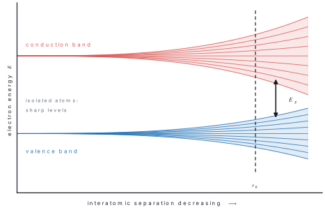
Two bands matter:
The valence band is the highest energy band that is completely or partly filled by the valence electrons of the atoms at 0\ \text{K}. The conduction band is the next allowed band above it; an electron in the conduction band is no longer tied to one atom and can drift through the whole crystal when a field is applied.
The energy range between the top of the valence band and the bottom of the conduction band contains no allowed states. It is the forbidden energy gap E_g.
A current flows only if electrons can gain small amounts of energy from the applied field, i.e. only if there are empty states immediately above occupied states. A completely full band carries no net current however strong the field, because every electron that moves one way is matched by one moving the other. This single sentence explains the whole of the next section.
25.2 Difference between metals, insulators and semi-conductors using band theory
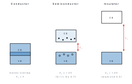
Conductors (metals). The valence band is only partly filled (sodium), or a filled valence band overlaps the empty conduction band (magnesium, zinc). Either way there is no gap: empty states sit immediately above occupied ones, a huge number of free electrons (\sim 10^{28}\ \text{m}^{-3}) is available, and the resistivity is tiny.
Insulators. The valence band is completely full, the conduction band completely empty, and E_g is large — 5.47\ \text{eV} for diamond. At 300\ \text{K} the average thermal energy of a particle is only about kT \approx 0.026\ \text{eV}, so practically no electron can be lifted across.
Semiconductors. The band picture is the same as an insulator's, but E_g is small: 1.1\ \text{eV} for silicon, 0.7\ \text{eV} for germanium. At 0\ \text{K} a semiconductor is a perfect insulator. At room temperature a small fraction of the bonds break, electrons jump the gap into the conduction band and leave holes behind in the valence band, and conduction begins.
| Property | Conductor | Semiconductor | Insulator |
|---|---|---|---|
| Forbidden gap E_g | zero (bands overlap) | \leq 3\ \text{eV} (Ge 0.7, Si 1.1) | > 3\ \text{eV} (diamond 5.47) |
| Resistivity at 300 K | 10^{-8}–10^{-6}\ \Omega\,\text{m} | 10^{-5}–10^{6}\ \Omega\,\text{m} | 10^{8}–10^{16}\ \Omega\,\text{m} |
| Carrier density | \sim 10^{28}\ \text{m}^{-3} | 10^{16}–10^{19}\ \text{m}^{-3} | negligible |
| Temperature coefficient of resistance | positive | negative | negative |
| Behaviour at 0\ \text{K} | still conducts | perfect insulator | perfect insulator |
| Examples | Cu, Ag, Al | Si, Ge, GaAs | diamond, mica, glass |
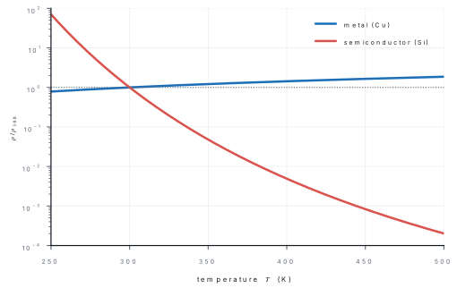
The negative temperature coefficient is the giveaway property of a semiconductor. Heating a metal makes the lattice ions vibrate more, electrons are scattered more often, and resistance rises. Heating a semiconductor does that too, but it also breaks far more bonds. In a pure semiconductor the Fermi level (the energy at which a state is half likely to be occupied) sits in the middle of the gap, so on the Boltzmann scale an electron only has to climb E_g/2 to reach the conduction band. The number of carriers therefore grows like e^{-E_g/2kT}, and this exponential growth easily overwhelms the extra scattering, so the resistivity falls.
Problem. The forbidden gap of silicon is 1.1\ \text{eV}. Find the longest wavelength of light that can lift an electron from its valence band into its conduction band. Take h = 6.63\times10^{-34}\ \text{J s}, c = 3\times10^{8}\ \text{m s}^{-1}, e = 1.6\times10^{-19}\ \text{C}.
Solution. One photon carries energy hc/\lambda. A long wavelength means a small energy, so the longest usable wavelength is the one whose photon energy is exactly E_g:
Make \lambda_{\max} the subject by cross-multiplying:
First change E_g from electron-volts to joules by multiplying by the electronic charge:
Next work out the numerator hc:
Now divide:
That is 1130\ \text{nm}, in the infrared. Visible light (400–700 nm) has a shorter wavelength and therefore more energy than this, which is why a silicon solar cell works in sunlight.
25.3 Intrinsic and extrinsic semi-conductors
Intrinsic semiconductors
A pure semiconductor is called intrinsic. Silicon and germanium are tetravalent: each atom shares its four valence electrons in covalent bonds with four neighbours, so at 0\ \text{K} every bond is complete and the crystal does not conduct.
At room temperature thermal energy breaks a few bonds. Each broken bond frees one electron into the conduction band and leaves behind a vacancy in the valence band — a hole. A neighbouring bound electron can hop into the vacancy, moving the vacancy the other way, so the hole behaves like a mobile particle of charge +e.
Because carriers are created only in pairs,
where n_i is the intrinsic carrier concentration: 1.5\times10^{16}\ \text{m}^{-3} for Si and 2.4\times10^{19}\ \text{m}^{-3} for Ge at 300\ \text{K}. Compare this with roughly 5\times10^{28} silicon atoms per cubic metre: only about one atom in 10^{12} contributes a carrier.
Step 1 — put the sample in a field. Take a bar of cross-section A and apply an electric field E along it. By the definition of mobility, the average (drift) speed a carrier picks up is mobility \times field:
Step 2 — count the electrons that cross a line in time t. Every electron within a distance v_e t of a chosen cross-section will reach it in time t. That slab has volume A v_e t, so the number of electrons in it is
Step 3 — turn that into charge, then into current. Each electron carries charge e, so the charge crossing is q = e\,n_e A v_e t. Current is charge per unit time, so divide by t:
Step 4 — divide by the area to get current density.
Step 5 — put the drift speed of Step 1 back in.
Step 6 — do the same for holes. Holes drift the opposite way but carry the opposite (positive) charge, so their current points the same way as the electron current and the two simply add:
Step 7 — add and take out the common factors e and E.
Step 8 — compare with Ohm's law. In point form Ohm's law reads J = \sigma E. Comparing the two expressions for J, the bracket must be the conductivity:
Step 9 — specialise to a pure sample. Putting n_e = n_h = n_i and taking n_i out as a common factor,
Here \mu_e and \mu_h are the electron and hole mobilities (drift velocity per unit field, in m² V⁻¹ s⁻¹). Electrons move through the lattice more easily than holes, so \mu_e > \mu_h always.
Problem. For intrinsic germanium at 300\ \text{K}, n_i = 2.4\times10^{19}\ \text{m}^{-3}, \mu_e = 0.39\ \text{m}^{2}\,\text{V}^{-1}\text{s}^{-1} and \mu_h = 0.19\ \text{m}^{2}\,\text{V}^{-1}\text{s}^{-1}. Find its conductivity and resistivity.
Solution. The sample is pure, so n_e = n_h = n_i and Step 9 above applies:
Add the two mobilities first:
Now multiply e by n_i. The powers of ten cancel (10^{-19}\times10^{19} = 10^{0} = 1):
Multiply the two results:
Finally invert to get resistivity:
This lies neatly between copper (1.7\times10^{-8}\ \Omega\,\text{m}) and glass.
Extrinsic semiconductors
Intrinsic material is far too resistive to be useful. Adding a controlled trace of impurity — typically one atom in 10^{6} to 10^{8} — is called doping, and the result is an extrinsic semiconductor.
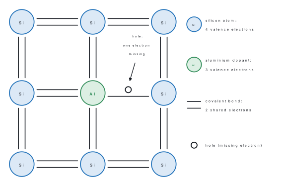
n-type. Dope silicon with a pentavalent atom (P, As, Sb, Bi). The impurity takes the place of a silicon atom in the lattice. Four of its five valence electrons pair up with electrons of the four silicon neighbours and make four ordinary covalent bonds. The fifth electron has no partner to bond with. It is held only weakly by its parent atom, and about 0.045\ \text{eV} in silicon (about 0.01\ \text{eV} in germanium) is enough to set it free — far less than the 1.1\ \text{eV} needed to break a bond. Since kT \approx 0.026\ \text{eV} at 300\ \text{K}, practically every impurity atom has already given up its fifth electron at room temperature. The impurity donates an electron, so it is called a donor, and electrons become the majority carriers.
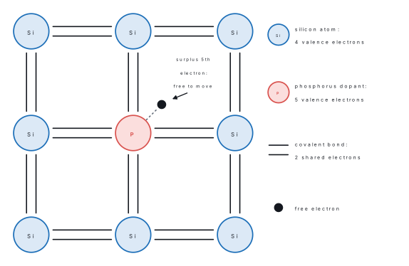
p-type. Dope silicon with a trivalent atom (B, Al, Ga, In). This atom brings only three valence electrons, so it can complete only three of the four bonds with its silicon neighbours. The fourth bond is left with a single electron instead of a pair. That empty half-bond is a hole. A bound electron from a neighbouring bond needs only about 0.05\ \text{eV} to jump across and fill it, which moves the hole to where that electron came from. Because the impurity accepts an electron it is called an acceptor, and holes become the majority carriers.
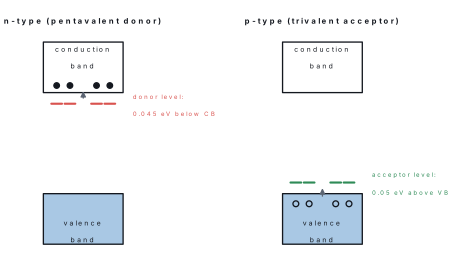
In band language the two dopants create new allowed levels inside the forbidden gap. A donor level sits only 0.045\ \text{eV} below the bottom of the conduction band, so its electron needs almost no help to get in. An acceptor level sits only about 0.05\ \text{eV} above the top of the valence band, so a valence electron can hop up into it and leave a hole behind.
Step 1 — what makes carriers. Heat breaks bonds and creates electron–hole pairs. How fast pairs appear (the generation rate g) depends only on the temperature and the gap E_g — it does not care how much impurity we added.
Step 2 — what destroys carriers. A free electron disappears only when it meets a hole and drops into it. The chance of a meeting is proportional to how many electrons there are and to how many holes there are, so the recombination rate is
where C is a constant fixed by the material and the temperature.
Step 3 — steady state. At a fixed temperature the carrier numbers are not changing, so pairs must be destroyed exactly as fast as they are made:
Step 4 — make the product the subject. Divide both sides by C:
The right-hand side contains only g and C, and both depend on temperature alone. So the product n_e n_h is the same number for every sample of that material at that temperature, however it is doped.
Step 5 — evaluate that number using the pure sample. In pure material at the same temperature, n_e = n_h = n_i, so
Step 6 — combine. Since the product is the same for all doping levels and equals n_i^2 for the pure sample, it must equal n_i^2 always:
So doping to raise one carrier density automatically suppresses the other: push n_e up by a factor of a million and n_h falls by the same factor.
| Feature | n-type | p-type |
|---|---|---|
| Dopant valency | pentavalent (P, As, Sb) | trivalent (B, Al, Ga, In) |
| Bonds formed by dopant | 4 complete bonds + 1 spare electron | 3 complete bonds + 1 hole |
| Impurity level created | donor, just below CB | acceptor, just above VB |
| Majority carriers | electrons | holes |
| Minority carriers | holes | electrons |
| Carrier relation | n_e \gg n_h, n_e \approx N_d | n_h \gg n_e, n_h \approx N_a |
| Net charge on crystal | zero | zero |
"n-type is negatively charged" is wrong, and it costs marks every year. A donor atom releases one electron but is left as a fixed positive ion, so the totals still balance. The labels n and p name the majority carrier, not a charge on the block.
A hole is the absence of an electron in a bond — a bookkeeping device for the motion of the many remaining valence electrons. It exists only inside the crystal, whereas a positron is a real particle that can travel through vacuum.
Problem. Pure silicon has n_i = 1.5\times10^{16}\ \text{m}^{-3} at 300\ \text{K}. It is doped with 10^{22} donor atoms per m³, all ionised. Find the electron and hole concentrations, and say which are the minority carriers.
Solution. Every ionised donor hands one electron to the conduction band, and N_d = 10^{22} is far bigger than n_i = 1.5\times10^{16}, so the thermally generated electrons are negligible in comparison:
Now use the law of mass action, n_e n_h = n_i^2. Make n_h the subject by dividing both sides by n_e:
Square n_i first — square the number and double the power of ten:
Then divide, subtracting the powers of ten (32 - 22 = 10):
Holes are the minority carriers. Note that one impurity atom per 5\times10^{6} silicon atoms has raised the electron density by a factor of about 10^{6} — that is the whole point of doping.
Chapter summary
- Bringing N atoms together splits each sharp atomic level into N levels so close (\sim 10^{-29}\ \text{eV} apart) that they form a continuous energy band; between bands lie forbidden gaps.
- The valence band is the highest band filled at 0\ \text{K}; the conduction band is the empty band above it; their separation is E_g.
- A completely filled band carries no current. Conduction needs empty states just above occupied ones.
- Conductor: bands overlap, E_g = 0. Semiconductor: E_g \leq 3\ \text{eV} (Ge 0.7 eV, Si 1.1 eV). Insulator: E_g > 3\ \text{eV} (diamond 5.47 eV).
- Semiconductors have a negative temperature coefficient of resistance because carrier number grows like e^{-E_g/2kT}.
- Intrinsic: n_e = n_h = n_i, and \sigma = e(n_e\mu_e + n_h\mu_h) reduces to \sigma_i = e\,n_i(\mu_e+\mu_h), with \rho = 1/\sigma.
- Extrinsic: a pentavalent dopant makes four bonds and leaves one spare electron (n-type, donor level below CB, electrons majority); a trivalent dopant makes three bonds and leaves one hole (p-type, acceptor level above VB, holes majority). Both crystals remain electrically neutral.
- Law of mass action: n_e n_h = n_i^{2} at a given temperature.
Practice questions
Group A — Multiple choice (1 mark each)
- In an intrinsic semiconductor at room temperature [1]an_e > n_hbn_e < n_hcn_e = n_hdn_h = 0
- The forbidden energy gap of germanium is about [1]a0.7\ \text{eV}b1.1\ \text{eV}c3.0\ \text{eV}d5.5\ \text{eV}
- On heating a semiconductor its resistance [1]aincreasesbdecreasescstays constantdfirst rises then falls
- Silicon doped with indium becomes [1]an-typebp-typecintrinsicdan insulator
- A pure semiconductor at 0\ \text{K} behaves as [1]aa conductorba superconductorca perfect insulatordan n-type semiconductor
- In n-type silicon the phosphorus atom forms [1]a5 covalent bondsb4 covalent bonds and has 1 spare electronc3 covalent bonds and 1 holedno bonds
Answers to Group A
1. (c) — carriers are produced only in electron–hole pairs.
2. (a) — Ge 0.7 eV, Si 1.1 eV.
3. (b) — the exponential rise in carrier number beats the extra scattering.
4. (b) — indium is trivalent, so it supplies acceptor levels.
5. (c) — every covalent bond is intact, so both bands are full or empty.
6. (b) — silicon offers only four neighbours, so the fifth electron of P has no bond to join.
Group B — Short answer (5 marks each)
- Explain qualitatively how the discrete energy levels of isolated atoms become energy bands in a solid. [5]
- Using band diagrams, distinguish between a conductor, a semiconductor and an insulator. [5]
- Why does the resistance of a metal increase but that of a semiconductor decrease with rise in temperature? [5]
- The energy gap of a certain semiconductor is 0.72\ \text{eV}. Calculate the maximum wavelength of radiation it can absorb. (h = 6.63\times10^{-34}\ \text{J s}) [5]
- Intrinsic silicon has n_i = 1.5\times10^{16}\ \text{m}^{-3}. After doping, the hole concentration becomes 4.5\times10^{21}\ \text{m}^{-3}. Find the electron concentration and name the type of the semiconductor. [5]
- Draw the covalent-bond diagram of silicon doped with a pentavalent atom and use it to explain why the material is called n-type although the crystal as a whole is neutral. [5]
Answers to Group B
1. Outline: sharp levels in an isolated atom → Pauli exclusion forbids N identical states → overlapping of outer orbitals on bringing N atoms together splits each level into N sub-levels → with N \sim 10^{29}\ \text{m}^{-3} the spacing is \sim 10^{-29}\ \text{eV}, so the set is effectively a continuous band, separated from the next by a forbidden gap.
3. Outline: in a metal the carrier number is fixed, so more violent lattice vibrations scatter electrons more and \rho rises. In a semiconductor the carrier number grows like e^{-E_g/2kT}; this exponential increase dominates the extra scattering, so \rho falls (negative temperature coefficient).
4. First convert the gap to joules:
Then \lambda_{\max} = hc/E_g with hc = 1.989\times10^{-25}\ \text{J m}:
5. By the law of mass action, n_e = n_i^2 / n_h. Square n_i first:
Then divide:
Holes greatly outnumber electrons, so the material is p-type.
6. Outline: draw the lattice of the n-type figure — P on a silicon site, four double-line covalent bonds to four Si neighbours, one extra electron drawn outside any bond. That spare electron is easily freed (0.045 eV), so electrons are the majority carriers and the material is called n-type. But the phosphorus atom that lost the electron is left behind as a fixed positive ion inside the lattice, so the positive and negative charges still balance exactly and the block is neutral.
Group C — Long answer (8 marks each)
- (a) Define valence band, conduction band and forbidden energy gap. [3](b) Draw band diagrams for a conductor, a semiconductor and an insulator and use them to explain the enormous difference in their resistivities. [5]
- (a) Distinguish between intrinsic and extrinsic semiconductors. [2](b) Draw the covalent-bond lattice of n-type and p-type silicon, showing the free electron and the hole, and name the majority carriers in each. [4](c) A germanium sample has n_i = 2.4\times10^{19}\ \text{m}^{-3}, \mu_e = 0.39 and \mu_h = 0.19\ \text{m}^{2}\text{V}^{-1}\text{s}^{-1}. Find the resistivity of the pure sample. [2]
Answer to Group C question 2(c)
Add the mobilities: \mu_e + \mu_h = 0.39+0.19 = 0.58. Then
Practise more: Physics question bank